Service hotline
+86 0755-83044319

release time:2025-06-03Author source:SlkorBrowse:5092
As miniaturized electronic systems evolve toward higher integration and lower power consumption, the synergistic innovation of piezoelectric MEMS (Micro-Electro-Mechanical Systems) technology and semiconductor devices is becoming a key breakthrough in the field of smart hardware. This paper takes the SD36C electrostatic protection diode as a starting point to explore its technological value and practical applications in the protection systems of piezoelectric MEMS devices.
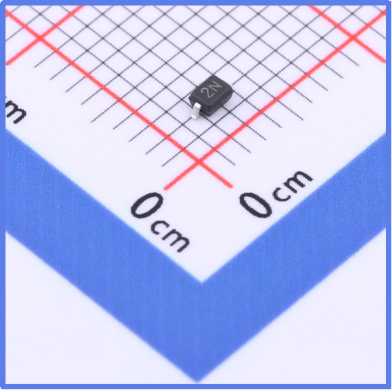
Slkor Electrostatic Discharge Diode SD36C product photo
As a core branch of micro-nano manufacturing technology, piezoelectric MEMS enables precise conversion between mechanical energy and electrical energy through the piezoelectric effect. It demonstrates unique advantages in sensors, actuators, and energy harvesting fields. The technological evolution of piezoelectric MEMS presents two major features:
● Materials Science Breakthroughs: The deposition processes for new piezoelectric thin films, such as lead zirconate titanate (PZT) and aluminum nitride (AlN), have matured, improving device energy density by over 30%. Additionally, the operating temperature range has been extended from -40°C to 150°C, meeting the demands of harsh environments such as automotive electronics.
● Structural Innovation: Microstructural designs, such as three-dimensional cantilever beams and multimodal resonators, combined with deep reactive ion etching (DRIE) processes, have reduced device feature sizes to the 1μm level. For example, the frequency response range of piezoelectric MEMS microphones now spans 20Hz to 80kHz, with a signal-to-noise ratio improved to 72dB.
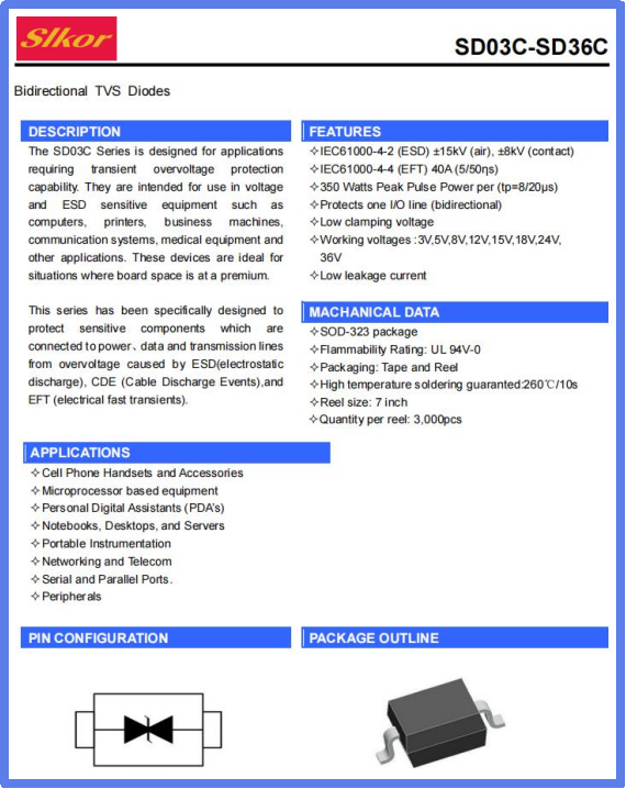
Slkor Electrostatic Discharge Diode SD36C specification
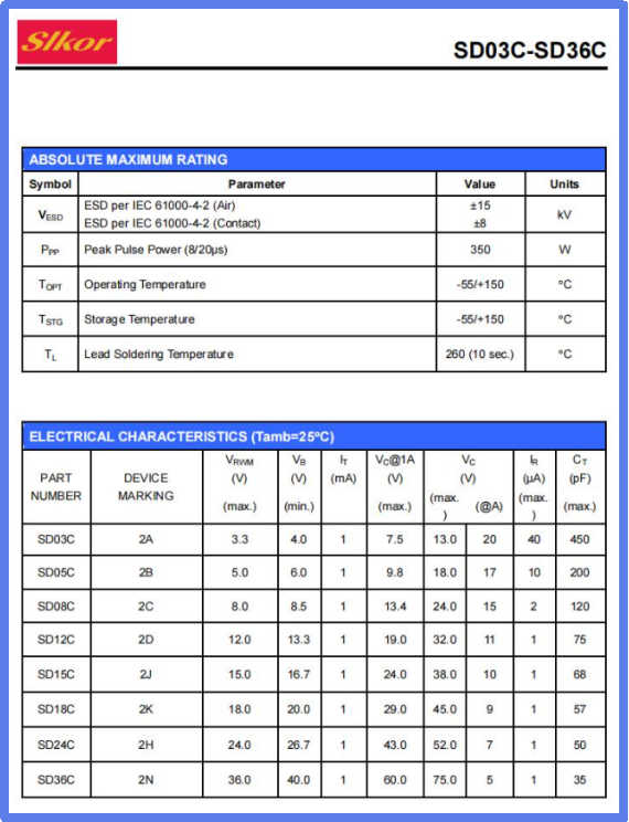
Parameters of Slkor Electrostatic Discharge Diode SD36C
As an electrostatic protection device designed for high-speed interfaces, the electrical characteristics of the SD36C (SOD-323 package) directly reflect its protection capabilities:
● VRWM=36V: This defines the transparency of the device to signal transmission under normal operating conditions, ensuring the integrity of high-speed bus signals, such as USB3.2 Gen2 (10Gbps). The typical insertion loss at the 5GHz frequency band is less than 0.3dB.
● VBR min=40V: This represents the minimum clamping voltage, providing a safety margin with respect to the breakdown voltage of piezoelectric MEMS devices. Experimental data show that, under IEC 61000-4-2 contact discharge at 8kV, the SD36C can control the output distortion rate of piezoelectric accelerometers to within 2%.
● CJ=35pF: The low junction capacitance design is crucial. In 5G millimeter-wave front-end modules, this parameter ensures that the S21 parameter fluctuation is less than 0.5dB, maintaining phase accuracy in piezoelectric MEMS phase shifters to better than 1.2°.
● VC=60V: The clamping voltage characteristic directly relates to the damage threshold of the protected device. For example, in piezoelectric MEMS ultrasonic transducers, the SD36C increases the ESD energy dissipation efficiency to 92%, an improvement of 18 percentage points over traditional TVS diodes.
● Consumer Electronics: In the protection of bone-conduction sensors in TWS (True Wireless Stereo) headphones, the SD36C’s 0.4mm×0.8mm micro-package achieves eutectic bonding with the piezoelectric MEMS device, ensuring that the sound pressure level (SPL) fluctuation remains below 0.2dB under 0.5J ESD impact.
● Automotive Electronics Systems: For piezoelectric ceramic driving circuits in onboard LiDAR systems, the SD36C, certified by AEC-Q101, maintains a leakage current (IR) of less than 1μA during temperature cycling tests from -55°C to 125°C, ensuring long-term stability of phase modulation accuracy.
● Industrial IoT Nodes: In piezoelectric MEMS energy harvesting modules, the SD36C works in conjunction with vibration energy conversion units to provide voltage clamping in a wide range from -200V to +200V, improving the MTBF of self-powered sensor nodes to 15 years.
With the development of heterogeneous integration technology, devices like the SD36C are exhibiting three main evolutionary directions:
● Three-Dimensional Stacked Packaging: By using TSV (Through-Silicon Via) technology to achieve vertical interconnection with piezoelectric MEMS chips, parasitic inductance is reduced to the 0.3nH range, shortening the protection response time to 500ps.
● Intelligent Adaptive Design: Integration of temperature compensation and voltage monitoring functions allows the clamping voltage to dynamically adjust within a ±10% range according to environmental temperature, making it suitable for wearable devices in bending deformation scenarios.
● Material System Innovation: The adoption of two-dimensional materials like hexagonal boron nitride (h-BN) to replace traditional silicon-based structures is predicted to reduce junction capacitance to below 5pF, opening up protective pathways for terahertz-band piezoelectric MEMS devices.
In the era of the Internet of Everything, the deep integration of piezoelectric MEMS technology and advanced protective devices is reshaping the reliability boundaries of intelligent sensing systems. The engineering practices of the SD36C demonstrate that through multi-dimensional collaborative design at the device, circuit, and system levels, a perfect balance of miniaturization, high performance, and high reliability can be achieved, providing critical support for the innovative development of smart hardware.
Slkor has research and development offices in Busan, South Korea, Beijing, China, and Suzhou, China. Most of the wafer manufacturing and packaging and testing are carried out within China. The company employs and collaborates with individuals and organizations worldwide, with a laboratory for product performance and reliability testing and a central warehouse located at its headquarters in Shenzhen. Slkor has filed for over a hundred invention patents, offers more than 2,000 product models, and serves over ten thousand customers globally. Its products are exported to countries and regions including Europe, the Americas, Southeast Asia, and the Middle East, making it one of the rapidly growing semiconductor companies in recent years. With well-established management systems and streamlined workflows, Slkor has rapidly enhanced the brand awareness and reputation of its "SLKOR" brand through its outstanding quality and standardized services. Its product range includes three major series: diodes, transistors, and power devices, with recent introductions of new products such as Hall elements and analog devices, expanding its presence in sensors, Risc-v microcontrollers, and other product categories.


Site Map | 萨科微 | 金航标 | Slkor | Kinghelm
RU | FR | DE | IT | ES | PT | JA | KO | AR | TR | TH | MS | VI | MG | FA | ZH-TW | HR | BG | SD| GD | SN | SM | PS | LB | KY | KU | HAW | CO | AM | UZ | TG | SU | ST | ML | KK | NY | ZU | YO | TE | TA | SO| PA| NE | MN | MI | LA | LO | KM | KN
| JW | IG | HMN | HA | EO | CEB | BS | BN | UR | HT | KA | EU | AZ | HY | YI |MK | IS | BE | CY | GA | SW | SV | AF | FA | TR | TH | MT | HU | GL | ET | NL | DA | CS | FI | EL | HI | NO | PL | RO | CA | TL | IW | LV | ID | LT | SR | SQ | SL | UK
Copyright ©2015-2025 Shenzhen Slkor Micro Semicon Co., Ltd
