Service hotline
+86 0755-83044319

release time:2025-05-12Author source:SlkorBrowse:6112
As electronic devices become increasingly sophisticated, Electrostatic Discharge (ESD) has become an invisible threat to circuit reliability. From smartphones to IoT devices, and from high-speed data interfaces to wearable devices, the performance of ESD protection components directly impacts a product's market competitiveness. This article takes the SLESD5Z3V3 ESD protection diode from a specific brand as an example to analyze its key parameters and reveal how modern ESD protection devices achieve dual breakthroughs in both precision protection and signal integrity.
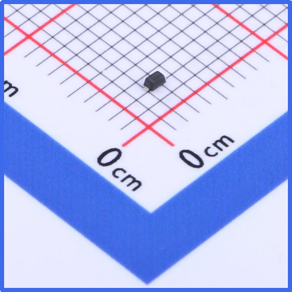
Slkor Electrostatic Discharge Diode SLESD5Z3V3 product photo
The SLESD5Z3V3 is an ESD protection device specifically designed for 3.3V low-voltage systems. It comes in an ultra-compact SOD-523 package (measuring only 1.6×0.8×0.5mm). Typical application scenarios include:
Mobile device USB/HDMI interfaces
High-speed data buses (such as MIPI, LVDS)
Portable medical electronics
IoT sensor nodes
The core design breakthrough lies in pushing beyond the performance limits of traditional TVS diodes. While ensuring compliance with IEC 61000-4-2 (±8kV contact discharge protection level), the junction capacitance (Cj) is reduced to 105pF, lowering it by more than 40% compared to similar products. This makes it perfectly suited for GHz-level high-speed signal transmission needs.
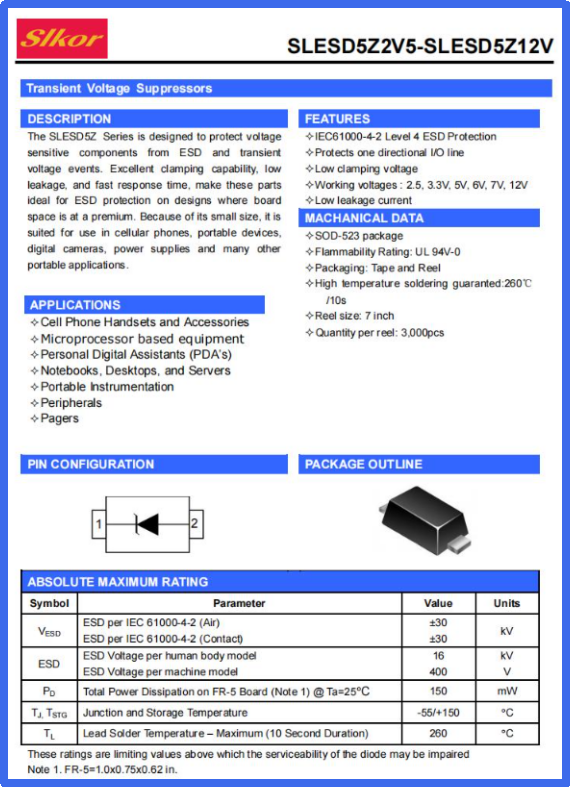
Slkor Electrostatic Discharge Diode SLESD5Z3V3 specification
1. Reverse Working Voltage (VRWM = 3.3V ±10%)
This parameter defines the device's normal operating voltage range. The 3.3V setting is precisely matched to mainstream digital circuit supply voltages, ensuring that the device remains in a high-impedance state (typical leakage current Ir = 0.9μA) across the full temperature range of -55°C to +150°C, without interfering with normal signal transmission. The ±10% tolerance effectively accommodates power supply fluctuations and avoids false triggering.
2. Breakdown Voltage (VBR min = 5V)
When the ESD pulse voltage exceeds 5V, the device enters avalanche breakdown mode, opening the ESD discharge channel. The strict control of the VBR min (±5% batch consistency) compared to the theoretical value prevents two failure modes:
A VBR too high leads to delayed protection and back-voltage surges damaging subsequent circuits.
A VBR too low causes increased normal leakage.
3. Clamping Voltage (VC = 9.4V @IPP = 1A)
Under the 8/20μs standard test waveform, when the surge current reaches 1A, the device limits the voltage to 9.4V. This parameter directly reflects the protection strength:
For CMOS devices powered by 3.3V, the VC must be below their gate oxide breakdown voltage (typically 12-15V).
Compared to traditional devices (VC ≈ 15V), the SLESD5Z3V3 reduces voltage stress by 37%.
4. Dynamic Characteristics Optimization
Junction Capacitance (Cj = 105pF @1MHz): Through a 3D electrode structure optimization, the parasitic capacitance is reduced to 60% of traditional devices, ensuring that insertion loss (S21) is below 0.5dB at 1GHz, meeting USB 3.1 Gen2 (10Gbps) transmission requirements.
Response Time (tr/tf < 1ns): Using a doping concentration gradient-controlled PN junction, the device achieves sub-nanosecond response times, effectively suppressing 1.2/50μs combo-wave interference as specified by IEC 61000-4-5.
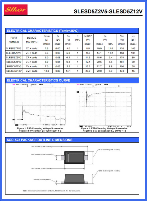
Parameters of Slkor Electrostatic Discharge Diode SLESD5Z3V3
1. High-Speed Interface Protection
In USB Type-C interfaces, the SLESD5Z3V3 can be parallel-connected to the D+/Ddifferential pairs. Its 105pF capacitance causes only 0.3dB attenuation at the 10GHz frequency band, ensuring that the eye diagram opening meets the specification. Actual tests show that under 5Gbps NRZ signals, the Bit Error Rate (BER) is better than 10^-12.
2. Power Rail Protection
For 3.3V power domains, it is recommended to use the bipolar device (SLESD5Z3V3B) for positive and negative ESD pulse protection. When laying out, follow these guidelines:
Place the device close to the connector (≤5mm).
Trace width ≥ 0.2mm to reduce parasitic inductance.
Avoid sharing ground loops with sensitive analog circuits.
3. Arrayed Applications
In HDMI 2.1 interfaces, using a 4-channel array package (SLESD5Z3V3-4) simplifies the layout. The isolation between channels is >30dB at 5GHz, effectively suppressing crosstalk.
Compared to traditional MLV (Multilayer Varistor) and Zener diode solutions, the SLESD5Z3V3 offers three key advantages:
1. Enhanced Protection Efficiency: Within the same package size, ESD protection capability is doubled (IEC 61000-4-2 level improved from ±4kV to ±8kV).
2. Signal Integrity Assurance: The breakthrough reduction in junction capacitance increases the data rate support capability from Mbps to Gbps.
3. System Cost Optimization: A single device can replace the traditional "TVS + ferrite bead" combination, reducing BOM costs by approximately 30%.
With the development of 5G, AIoT, and other technologies, ESD protection devices are showing two major trends:
Ultra-Low Capacitance: Products with 10pF capacitance have entered mass production.
Smart Integration: Intelligent protection chips with status monitoring are emerging.
The SLESD5Z3V3 ESD protection diode offers a reliable electrostatic protection solution for high-speed digital systems through precise balancing of its parameters. Its design concept reflects the industry's development trend: at the nanoscale process node, ESD protection devices have evolved from mere protective components to key elements in system design. For engineers, a deep understanding of the relationship between device parameters and system requirements will be the core competency in achieving high reliability and cost optimization in products.
Slkor has research and development offices in Busan, South Korea, Beijing, China, and Suzhou, China. Most of the wafer manufacturing and packaging and testing are carried out within China. The company employs and collaborates with individuals and organizations worldwide, with a laboratory for product performance and reliability testing and a central warehouse located at its headquarters in Shenzhen. Slkor has filed for over a hundred invention patents, offers more than 2,000 product models, and serves over ten thousand customers globally. Its products are exported to countries and regions including Europe, the Americas, Southeast Asia, and the Middle East, making it one of the rapidly growing semiconductor companies in recent years. With well-established management systems and streamlined workflows, Slkor has rapidly enhanced the brand awareness and reputation of its "SLKOR" brand through its outstanding quality and standardized services. Its product range includes three major series: diodes, transistors, and power devices, with recent introductions of new products such as Hall elements and analog devices, expanding its presence in sensors, Risc-v microcontrollers, and other product categories.


Site Map | 萨科微 | 金航标 | Slkor | Kinghelm
RU | FR | DE | IT | ES | PT | JA | KO | AR | TR | TH | MS | VI | MG | FA | ZH-TW | HR | BG | SD| GD | SN | SM | PS | LB | KY | KU | HAW | CO | AM | UZ | TG | SU | ST | ML | KK | NY | ZU | YO | TE | TA | SO| PA| NE | MN | MI | LA | LO | KM | KN
| JW | IG | HMN | HA | EO | CEB | BS | BN | UR | HT | KA | EU | AZ | HY | YI |MK | IS | BE | CY | GA | SW | SV | AF | FA | TR | TH | MT | HU | GL | ET | NL | DA | CS | FI | EL | HI | NO | PL | RO | CA | TL | IW | LV | ID | LT | SR | SQ | SL | UK
Copyright ©2015-2025 Shenzhen Slkor Micro Semicon Co., Ltd
