Service hotline
+86 0755-83044319

release time:2025-06-09Author source:SlkorBrowse:5244
In the digital era, data centres, as the core infrastructure supporting cloud computing, artificial intelligence and the Internet of Things (IoT), have a direct relationship between their stability and safety and the lifeblood of the digital economy. However, the complex electromagnetic environment and high-frequency signal transmission inside the data centre make electrostatic discharge (ESD) an invisible killer that threatens the reliability of hardware. Against this backdrop, the electrostatic protection diode SLESD8D12CT5G, with its excellent performance parameters and compact design, has become a key component in ensuring the stable operation of data centre infrastructure.
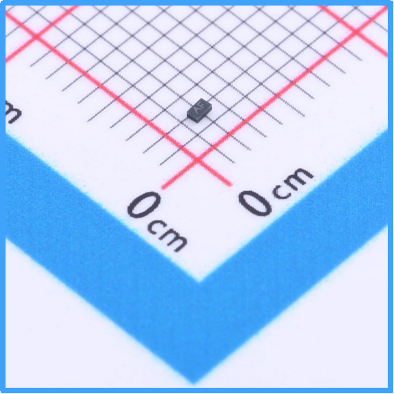
Slkor Electrostatic Discharge Diode SLESD8D12CT5G product photo
Modern data centre servers, storage devices and network switches commonly use high-speed serial interfaces (e.g. PCIe 5.0, 100G Ethernet), and their signal transmission rates have exceeded the tens of Gbps level. However, high-speed signals are extremely sensitive to electrostatic shocks: a small ESD event can lead to signal integrity failures, data transmission errors, and even permanent chip damage. According to statistics, the global annual loss of electronic equipment failure due to electrostatic up to billions of dollars, of which data centre scenarios account for a significant proportion.
Traditional protection solutions are limited by capacitive effect and response speed, difficult to meet the needs of high-frequency applications. The SLESD8D12CT5G is innovatively designed to achieve a minimum breakdown voltage of 14V (VBR min) at 12V operating voltage, which is compatible with low-voltage digital circuits and provides sufficient protection redundancy. Its ultra-low reverse leakage current (IR) of 0.01μA ensures near-zero quiescent power consumption and is perfectly suited to the stringent energy efficiency requirements of data centres.
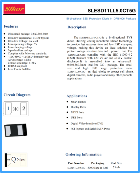
Slkor Electrostatic Discharge Diode SLESD8D12CT5G specification
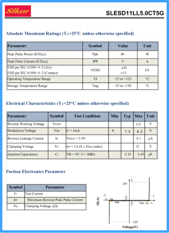
Parameters of Slkor Electrostatic Discharge Diode SLESD8D12CT5G
Bidirectional Protection Architecture
The device adopts a bi-directional conduction structure to suppress both positive and negative pulse impacts, which is particularly suitable for protection scenarios of differential signal lines (e.g. USB 3.2, HDMI 2.1). Its 19V clamp voltage (VC) design can limit the voltage peak to a safe threshold when an ESD event occurs, avoiding over-voltage damage to the back-end circuits.
Ultra-low junction capacitance (CJ=8pF)
Conventional TVS diodes can cause high-speed signal attenuation due to high parasitic capacitance (usually >50pF). SLESD8D12CT5G compresses the junction capacitance to the level of 8pF by optimising the semiconductor doping process, ensuring that the loss of signal integrity is less than 1dB in the 10GHz band, which makes it perfectly suitable for high-speed interfaces such as PCIe 5.0 (16GT/s). ) and other high-speed interfaces.
Miniature DFN1006 package
The package size is only 1.0mm x 0.6mm and thickness is 0.35mm, which is suitable for high-density PCB layout. On data centre server motherboards, as many as 12 ESD devices need to be arranged around a single U.2 interface. The DFN1006 package saves more than 40% of the board space and leaves more room for heat dissipation design.
Servers & Storage Systems
In NVMe SSD arrays, the SLESD8D12CT5G can be deployed in PCIe signal lines, SATA power ports, and LED status indicator circuits to protect against ESD shocks triggered by plug-and-play operations or human contact. Its 12V operating voltage (VRWM) is directly compatible with the server motherboard 12V power supply system without the need for additional voltage conversion circuitry.
Network Device Protection
High-speed differential pairs (Differential Pairs) in 25G/100G Ethernet optical modules are extremely sensitive to parasitic capacitance. The device's 8pF junction capacitance can increase the signal eye diagram opening by more than 30%, ensuring that the bit error rate (BER) is maintained at the 10^-12 order of magnitude to meet the needs of low-latency scenarios such as financial transactions.
Edge Computing Nodes
In distributed data centre architectures, edge servers are often deployed in industrial environments. The SLESD8D12CT5G is certified by IEC 61000-4-2 Contact Discharge 8kV/Air Discharge 15kV, which protects against strong static interference in industrial sites and guarantees stable operation of the equipment over a wide temperature range of -55℃ to +150℃.
Technology Evolution and Industry Trends
As data centres evolve to 400G/800G Ethernet, the signal rate will exceed 112Gbps, which poses the challenge of lower capacitance (<3pF) and faster response (<1ns) for ESD devices. subsequent iterations of the SLESD8D12CT5G have begun to adopt 3D packaging technology, further compressing parasitic parameters by vertically stacking the chips. parameters. Meanwhile, third-generation semiconductor solutions based on GaN materials are being developed to reduce clamp voltages to less than 15V, providing better protection for future CPO (co-packaged optics) architectures.
SLESD8D12CT5G electrostatic protection diode achieves ‘big action’ with ‘small body’ in the precision electronic system of data centre infrastructure. Each breakthrough in its technical parameters accurately solves the protection pain points in high-frequency, high-voltage and high-density scenarios. With the exponential growth of computing power demand for AI large model training, this kind of miniaturised, high-performance passive devices will become the cornerstone for building the ‘Great Wall of ESD’ in the digital world.
Slkor has research and development offices in Busan, South Korea, Beijing, China, and Suzhou, China. Most of the wafer manufacturing and packaging and testing are carried out within China. The company employs and collaborates with individuals and organizations worldwide, with a laboratory for product performance and reliability testing and a central warehouse located at its headquarters in Shenzhen. Slkor has filed for over a hundred invention patents, offers more than 2,000 product models, and serves over ten thousand customers globally. Its products are exported to countries and regions including Europe, the Americas, Southeast Asia, and the Middle East, making it one of the rapidly growing semiconductor companies in recent years. With well-established management systems and streamlined workflows, Slkor has rapidly enhanced the brand awareness and reputation of its "SLKOR" brand through its outstanding quality and standardized services. Its product range includes three major series: diodes, transistors, and power devices, with recent introductions of new products such as Hall elements and analog devices, expanding its presence in sensors, Risc-v microcontrollers, and other product categories.


Site Map | 萨科微 | 金航标 | Slkor | Kinghelm
RU | FR | DE | IT | ES | PT | JA | KO | AR | TR | TH | MS | VI | MG | FA | ZH-TW | HR | BG | SD| GD | SN | SM | PS | LB | KY | KU | HAW | CO | AM | UZ | TG | SU | ST | ML | KK | NY | ZU | YO | TE | TA | SO| PA| NE | MN | MI | LA | LO | KM | KN
| JW | IG | HMN | HA | EO | CEB | BS | BN | UR | HT | KA | EU | AZ | HY | YI |MK | IS | BE | CY | GA | SW | SV | AF | FA | TR | TH | MT | HU | GL | ET | NL | DA | CS | FI | EL | HI | NO | PL | RO | CA | TL | IW | LV | ID | LT | SR | SQ | SL | UK
Copyright ©2015-2025 Shenzhen Slkor Micro Semicon Co., Ltd
