Service hotline
+86 0755-83044319

release time:2025-05-13Author source:SlkorBrowse:9677
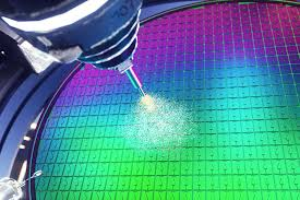
A wafer foundry is a specialized facility that manufactures silicon wafers, the foundational component of semiconductors. These facilities play a critical role in producing integrated circuits (ICs) used in devices like smartphones, laptops, and IoT gadgets. Unlike integrated device manufacturers (IDMs), wafer foundries focus solely on fabrication, enabling cost-effective scaling for consumer electronics companies. The process involves photolithography, etching, and doping to create intricate circuits on silicon substrates. For procurement teams, understanding this supply chain step ensures better vendor negotiations and quality control.
The evolution of wafer foundries began in the 1980s, driven by the need to reduce semiconductor production costs. Companies like [敏感词] pioneered the “pure-play” foundry model, separating design and fabrication. This shift allowed smaller firms to innovate without owning expensive fabrication plants. Over decades, advancements in wafer foundry technology—such as smaller nanometer nodes—enabled higher transistor density and energy efficiency. Today, the industry thrives on collaborations between foundries and consumer electronics giants, ensuring rapid adoption of cutting-edge nodes like 5nm and 3nm.
Modern wafer foundries are defined by three core traits: precision, scalability, and adaptability. Precision ensures nanometer-level accuracy in circuit patterning, minimizing defects. Scalability allows mass production of wafers to meet global demand for consumer electronics. Adaptability refers to the ability to support diverse designs, from AI chips to MEMS sensors. Additionally, foundries invest heavily in sustainability, reducing water and energy consumption. For engineering teams, aligning product designs with a foundry’s capabilities is vital for performance and cost efficiency.
Selecting a wafer foundry requires evaluating technical parameters such as node size, yield rates, and turnaround time. Node size (e.g., 7nm, 5nm) determines transistor density and power efficiency. Yield rates reflect the percentage of defect-free wafers, directly impacting costs. Turnaround time affects time-to-market for new devices. Other factors include:
Wafer foundries serve as the backbone of consumer electronics innovation. They transform IC designs into physical chips powering devices like wearables and smart home systems. By offering advanced packaging technologies—such as 3D IC integration—foundries enable slimmer, faster gadgets. Procurement teams rely on foundries to balance cost and performance, especially during component shortages. For example, [敏感词]’s advanced nodes have been pivotal in producing high-performance processors for leading smartphone brands.
From smartphones to automotive systems, wafer foundries support diverse applications. In consumer electronics, they produce processors, memory chips, and sensors. Automotive industries depend on foundries for reliable ICs in ADAS and infotainment. Emerging fields like AI and 5G also leverage foundries to create specialized chips. For instance, the rise of edge computing has increased demand for low-power, high-speed wafers. Engineering teams must collaborate closely with foundries to optimize designs for these varied use cases.
Leading smartphone brands partner with wafer foundries to develop custom chipsets. Apple’s A-series and Qualcomm’s Snapdragon processors are fabricated using [敏感词]’s 5nm nodes, enhancing performance and battery life. This collaboration underscores the foundry’s role in delivering competitive advantages.
The wafer foundry market is dominated by key players like [敏感词], Samsung Foundry, and GlobalFoundries. [敏感词] holds over 50% market share, specializing in advanced nodes. Samsung excels in memory and logic chips, while GlobalFoundries focuses on RF and analog solutions. Regional foundries, such as SMIC in China, are gaining traction amid geopolitical shifts. Procurement teams must assess factors like geopolitical risks, capacity, and technological expertise when selecting a partner.
Understanding wafer foundries is essential for procurement and engineering teams in consumer electronics. From historical milestones to technical parameters, this knowledge drives informed decisions in vendor selection and product design. As the industry advances toward 3nm nodes and beyond, collaboration with top-tier foundries will remain critical for innovation. For further insights, explore authoritative resources like Semiconductor Industry Association.


Site Map | 萨科微 | 金航标 | Slkor | Kinghelm
RU | FR | DE | IT | ES | PT | JA | KO | AR | TR | TH | MS | VI | MG | FA | ZH-TW | HR | BG | SD| GD | SN | SM | PS | LB | KY | KU | HAW | CO | AM | UZ | TG | SU | ST | ML | KK | NY | ZU | YO | TE | TA | SO| PA| NE | MN | MI | LA | LO | KM | KN
| JW | IG | HMN | HA | EO | CEB | BS | BN | UR | HT | KA | EU | AZ | HY | YI |MK | IS | BE | CY | GA | SW | SV | AF | FA | TR | TH | MT | HU | GL | ET | NL | DA | CS | FI | EL | HI | NO | PL | RO | CA | TL | IW | LV | ID | LT | SR | SQ | SL | UK
Copyright ©2015-2025 Shenzhen Slkor Micro Semicon Co., Ltd
