Service hotline
+86 0755-83044319

release time:2025-06-21Author source:SlkorBrowse:6371
As RF (Radio Frequency) technology advances towards higher frequencies and increased integration, Electrostatic Discharge (ESD) has become a hidden threat to the reliability of RF modules. The fragility and high-frequency characteristics of RF signals make them highly sensitive to transient high voltages, parasitic capacitance, and electromagnetic interference (EMI) caused by ESD. The SLESD2401QC ESD protection diode, launched by Slkor, offers a reliable ESD protection solution for RF products, thanks to its ultra-low capacitance, high response speed, and miniaturized packaging. This article will analyze its key role in the RF field from three perspectives: technical characteristics, RF application scenarios, and domestic production value.
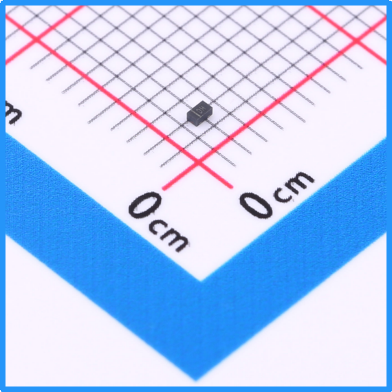
Slkor Electrostatic Discharge Diode SLESD2401QC product photo
RF products are widely used in 5G base stations, satellite communications, radar systems, and consumer electronics (e.g., Wi-Fi 6E routers, smartphones). The core challenges include:
1. High Frequency Signal Attenuation: Traditional ESD devices with high junction capacitance (>50pF) significantly attenuate GHz-level RF signals, leading to increased insertion loss.
2. Transient High Voltage Damage: ESD pulse voltages can reach thousands of volts and may break down the gate oxide layer of RF front-end chips (e.g., LNA, PA).
3. Space and Heat Dissipation Constraints: RF module PCBs are compact, and extra heat dissipation caused by protective devices must be minimized.
The DFN1006 package (1.0mm×0.6mm×0.37mm) of SLESD2401QC, along with its 13pF ultra-low junction capacitance, is designed to address these challenges.
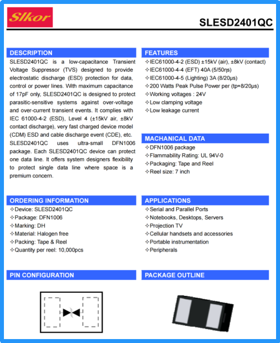
Slkor Electrostatic Discharge Diode SLESD2401QC specification
The key parameters and RF compatibility of the SLESD2401QC are as follows:
● VRWM (Reverse Working Voltage): 24V, suitable for the DC bias voltage of mainstream RF chips (e.g., 12V~28V power supply range for 5G NR modules).
● VBR min (Breakdown Voltage): 26V, ensuring no conduction under normal operating voltage to prevent signal leakage.
● VC (Clamping Voltage): 36V, quickly clamping the voltage to a safe range under ESD impact, protecting the downstream chips.
● CJ (Junction Capacitance): 13pF, reducing RF signal attenuation by more than 70% compared to traditional TVS diodes (>50pF).
● IR (Reverse Leakage Current): 1μA, maintaining low power consumption even at high temperatures (85°C) to avoid thermal effects impacting RF performance.
● Packaging Advantages: The DFN1006 package supports SMT reflow soldering and is compatible with high-density PCB designs.
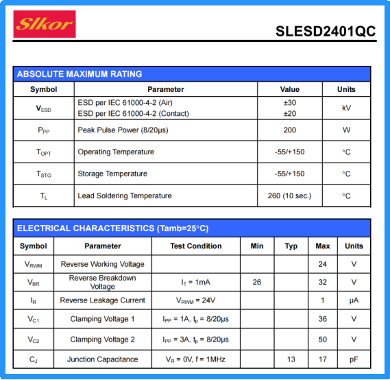
Parameters of Slkor Electrostatic Discharge Diode SLESD2401QC
1. 5G Base Station RF Front-End Protection
In 5G Massive MIMO antenna arrays, the SLESD2401QC protects the LNA (Low Noise Amplifier) and PA (Power Amplifier) of each RF channel. For instance, in domestically produced 700MHz band 5G base stations, the 13pF junction capacitance of this device can control insertion loss to within 0.2dB, while withstanding ±8kV contact discharge impacts under IEC 61000-4-2 standards.
2. Satellite Communication Terminal Protection
In Ka/Ku band satellite communication modules, SLESD2401QC can be embedded between the antenna interface and RF transceivers. For example, in domestically produced portable satellite terminals, its ultra-low capacitance property prevents attenuation of signals above 20GHz, while its bidirectional protection function safeguards against electrostatic and radiation interference in space.
3. Consumer Electronics RF Interface Protection
In devices such as smartphones and Wi-Fi 6E routers, SLESD2401QC protects high-speed RF coexistence circuits like USB 3.2 and HDMI 2.1 interfaces. For instance, in domestically produced 5G smartphones, its miniaturized package fits limited PCB space and reduces interference to Wi-Fi 6E (6GHz band) signals.
1. Matching Design with RF Chips
The VRWM (24V) and VBR min (26V) of SLESD2401QC must be coordinated with the DC bias voltage of RF chips. For example, in GaN-based PAs, the breakdown voltage of the protection device must be higher than the maximum gate voltage of the chip (typically 25V~28V).
2. Parasitic Parameter Simulation and Optimization
Electromagnetic simulation tools such as HFSS can be used to optimize the layout of SLESD2401QC in the RF path. For instance, placing the device close to the antenna interface and shortening trace lengths can further reduce parasitic inductance (<0.5nH) and minimize high-frequency signal reflections.
3. Multi-Level Protection Architecture
For ultra-high-frequency applications, SLESD2401QC can be combined with gas discharge tubes (GDTs) for protection. For instance, in domestically produced millimeter-wave radar (77GHz), SLESD2401QC responds to ESD pulses (in nanoseconds), while the GDT absorbs the subsequent surge energy.
The launch of SLESD2401QC marks a significant leap for domestic RF protection devices from "usable" to "highly effective." Against the backdrop of rapid development in RF technologies such as 5G, satellite communications, and IoT, its ultra-low capacitance, high reliability, and miniaturized features provide an invisible yet crucial protective barrier for RF products. As domestic RF chips and modules continue to evolve, SLESD2401QC and its successor products will further push the boundaries of RF protection technology, helping China secure a technological edge in the global RF industry.


Site Map | 萨科微 | 金航标 | Slkor | Kinghelm
RU | FR | DE | IT | ES | PT | JA | KO | AR | TR | TH | MS | VI | MG | FA | ZH-TW | HR | BG | SD| GD | SN | SM | PS | LB | KY | KU | HAW | CO | AM | UZ | TG | SU | ST | ML | KK | NY | ZU | YO | TE | TA | SO| PA| NE | MN | MI | LA | LO | KM | KN
| JW | IG | HMN | HA | EO | CEB | BS | BN | UR | HT | KA | EU | AZ | HY | YI |MK | IS | BE | CY | GA | SW | SV | AF | FA | TR | TH | MT | HU | GL | ET | NL | DA | CS | FI | EL | HI | NO | PL | RO | CA | TL | IW | LV | ID | LT | SR | SQ | SL | UK
Copyright ©2015-2025 Shenzhen Slkor Micro Semicon Co., Ltd
