Service hotline
+86 0755-83044319

release time:2025-05-12Author source:SlkorBrowse:9005
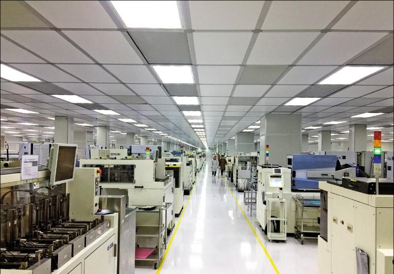
A Semiconductor Assembly and Testing Facility, or semiconductor assembly and testing facility, plays a critical role in the electronics manufacturing ecosystem. These facilities specialize in the final stages of semiconductor production, including packaging integrated circuits (ICs) and rigorously testing their functionality. For procurement and engineering teams in consumer electronics, understanding the capabilities of a Semiconductor Assembly and Testing Facility ensures efficient supply chain management and product reliability.
The evolution of Semiconductor Assembly and Testing Facility dates back to the 1960s, when the semiconductor industry began transitioning from discrete components to ICs. Early facilities focused on simple packaging methods like Dual In-line Packages (DIP). Over decades, advancements in miniaturization and automation transformed Semiconductor Assembly and Testing Facility into highly sophisticated hubs. Today, they employ cutting-edge technologies such as 3D packaging and system-in-package (SiP) designs. This progression aligns with the growing complexity of consumer electronics, as detailed in industry reports.
Modern Semiconductor Assembly and Testing Facility are defined by several distinctive features:
· High Precision Equipment: Tools for wire bonding and flip-chip assembly ensure micron-level accuracy.
· Advanced Testing Systems: Automated testers validate performance under extreme conditions.
· Scalability: Facilities adapt to fluctuating demand for consumer electronics components.
When evaluating a Semiconductor Assembly and Testing Facility, engineers prioritize metrics like yield rate, thermal management, and signal integrity. For instance, a yield rate above 98% minimizes material waste, while robust thermal designs prevent overheating in compact devices like smartphones.
The Semiconductor Assembly and Testing Facility bridges the gap between wafer fabrication and end-product integration. Key responsibilities include:
· Protecting delicate ICs from environmental damage.
· Ensuring electrical connectivity through precise pin layouts.
· Identifying defects before components reach assembly lines.
From smartphones to smart home devices, Semiconductor Assembly and Testing Facility enable the mass production of reliable ICs. For example, 5G chipsets require specialized testing for high-frequency performance, while IoT sensors demand ultra-low-power validation. These applications underscore the Semiconductor Assembly and Testing Facility's role in meeting market-driven innovation.
Prominent players like ASE Technology and Amkor Technology dominate the global Semiconductor Assembly and Testing Facility landscape. These firms invest heavily in R&D to support emerging trends such as artificial intelligence processors and automotive-grade ICs. Procurement teams often prioritize partners with certifications like IATF 16949 for automotive compliance.
Key considerations include technical expertise, geographic proximity to assembly plants, and adherence to ethical sourcing practices. A rigorous audit process helps mitigate risks in the supply chain.
The rise of heterogeneous integration and chiplets is reshaping Semiconductor Assembly and Testing Facility operations. Innovations like fan-out wafer-level packaging (FOWLP) allow tighter component integration, addressing demands for smaller, faster devices. Staying ahead of these trends is vital for engineering teams aiming to optimize product designs.
As consumer electronics evolve, the Semiconductor Assembly and Testing Facility remains indispensable in delivering high-performance, reliable components. By mastering its functions, parameters, and industry trends, procurement and engineering teams can drive efficiency and innovation. For further insights, explore resources from the Semiconductor Industry Association.


Site Map | 萨科微 | 金航标 | Slkor | Kinghelm
RU | FR | DE | IT | ES | PT | JA | KO | AR | TR | TH | MS | VI | MG | FA | ZH-TW | HR | BG | SD| GD | SN | SM | PS | LB | KY | KU | HAW | CO | AM | UZ | TG | SU | ST | ML | KK | NY | ZU | YO | TE | TA | SO| PA| NE | MN | MI | LA | LO | KM | KN
| JW | IG | HMN | HA | EO | CEB | BS | BN | UR | HT | KA | EU | AZ | HY | YI |MK | IS | BE | CY | GA | SW | SV | AF | FA | TR | TH | MT | HU | GL | ET | NL | DA | CS | FI | EL | HI | NO | PL | RO | CA | TL | IW | LV | ID | LT | SR | SQ | SL | UK
Copyright ©2015-2025 Shenzhen Slkor Micro Semicon Co., Ltd
