Service hotline
+86 0755-83044319
release time:2023-10-14Author source:SlkorBrowse:13460
In 2022, the semiconductor market was approximately 0.6 trillion USD, and commercial analysts predict that it will double to 1.0-1.3 trillion USD by 2030. The significant growth in the semiconductor manufacturing industry can be seen in the lithography process. Lithography is a patterning process that transfers a flat design onto the surface of a wafer substrate, creating complex structures such as transistors and interconnects. This is accomplished by selectively exposing photosensitive polymers or photoresists to light of specific wavelengths through a complex multi-step process. Recent advancements in lithography technology have created a competitive advantage in the production of cutting-edge semiconductors, enabling advanced technologies such as artificial intelligence (AI), 5G telecommunications, and supercomputing. Therefore, advanced semiconductor technology has an impact on national security and economic prosperity.
Currently, the most advanced semiconductor lithography process uses EUV (Extreme Ultraviolet) light source, particularly at a wavelength of 13.5nm. EUV light allows for the construction of smaller unit features within semiconductors. It has been reported that the cost of EUVL systems is currently around 150 million USD, and it was first deployed by ASML in 2019, which maintains a 100% market share. So far, ASML has shipped three different models of EUVL systems, namely Twinscan NXE: 3400B/C and NXE: 3600D. The total shipments of NXE systems have increased from 31 units in the first quarter of 2019 to 181 units in the last quarter of 2022.
The organization of this report is as follows. The remaining part of the introduction includes the technical background of EUVL, the international and domestic status of EUVL, and an overview of the R&D measurement programs by NIST and CHIPS. Section 2 contains the discussion of the technical status and requirements of EUVL technology in the working group meetings. Section 3 outlines the survey results and recommendations for the way forward discussed in the working group meetings, concluding the report.
1.1 Technical Background of EUV Lithography
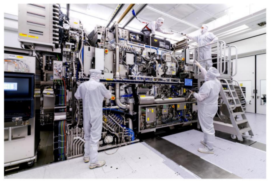
EUVL is a critical step in manufacturing next-generation semiconductor chips. EUV light is generated by a high-temperature plasma created from high-purity tin. Solid tin is melted in a droplet generator instrument that continuously produces over 3 million 27µm droplets per minute within a vacuum chamber. A pulsed 25kW average power carbon dioxide laser irradiates each tin droplet with two consecutive pulses to respectively form and ionize the droplet. Initially, kilowatts of EUV light are produced, but only a small fraction becomes lithographic exposure due to absorption and scattering losses along the light path. The output power and beam quality of 13.5nm light are inferred through indirect scintillator-camera measurements. A multilayer condenser system guides the light to the photosensitive area. The condenser system is protected from tin debris by a continuous flow of hydrogen gas. After each exposure, automatic chip-level positioning of the chip's resolution is verified to be ≤0.25nm through 20,000 cycles of inspection and adjustment per second. Overall, this process requires precise coordination among many different engineering systems. Figure 1 shows a photograph of ASML's EUVL components.
1.2 Current and Future State of EUV Lithography Technology
The growth in advanced semiconductor manufacturing comes from new EUV manufacturing facilities in the United States, Europe, and Asia. As previously mentioned, the only company currently producing EUVL scanner components is ASML, headquartered in the Netherlands. ASML sells EUV scanner components to companies such as Intel, [敏感词] Semiconductor Manufacturing Company ([敏感词]), and Samsung in their semiconductor manufacturing facilities. The EUVL system is not just created in the Netherlands but rather composed of many modules developed globally, then transported to ASML's headquarters in the Netherlands for final assembly and testing before delivery to customers.
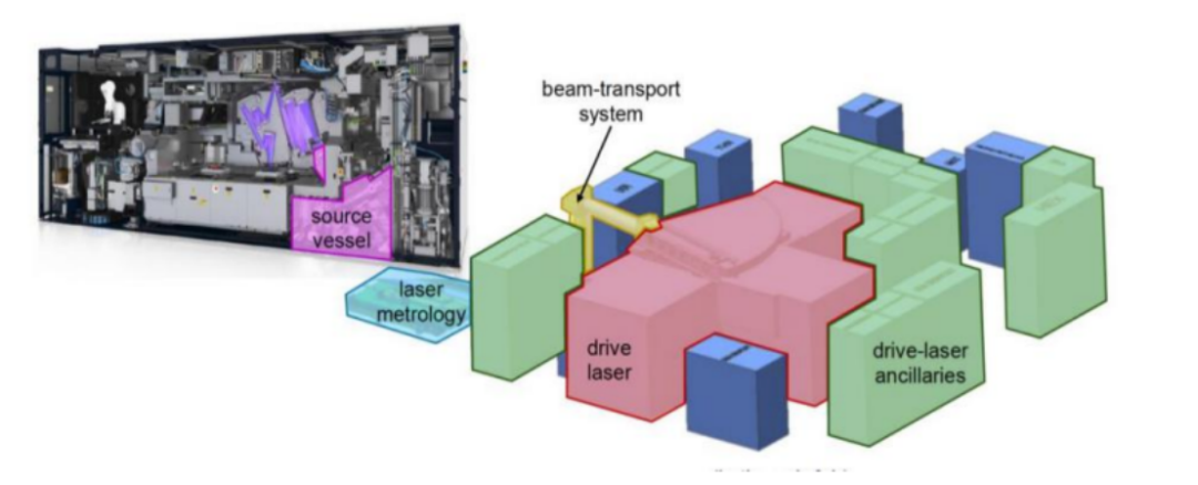
From the US perspective, research, development, and manufacturing of ASML's EUV source are based in San Diego, California. The light source component of the EUVL scanner assembly is shown in Figure 2. It should be noted that the light source component includes the source container located within the EUVL scanner assembly, as well as many components beneath the manufacturing floor, including laser metrology, beam transport systems, and drive lasers and their auxiliary equipment. The San Diego-based source operation is a result of ASML's acquisition of Cymer in 2012 to advance EUV source technology. Furthermore, given the advantages of EUVL in semiconductor manufacturing, export controls have recently protected this technology. Specifically, in October 2022, the Bureau of Industry and Security (BIS) issued a rule, 87FR62186, which includes the export control of technology, including Extreme Ultraviolet lithography (b.2).
ASML stated that the future development of EUV lithography technology includes increasing the numerical aperture (NA) from 0.33 to 0.55 ("high NA"). High NA can be used to reduce the number of multimode steps required by the current 0.33 NA and result in the resolution of finer geometries. This is consistent with the publicly released 2022 IEEE International Roadmap for Devices and Systems (IRDS), which requires transistor scaling to continue to 0.5nm by 2037. The goal of the new NA platform is to improve the speed of wafer and particle state, enabling the scaling of geometric chip features. High NA systems are expected to be shipped to customers in 2023 and achieve full production by 2025. In early 2023, ASML announced that they have achieved two new EUV power records, running at 600W EUV emission per hour, meeting the high NA EXE: 5200 dose stability specification and 700W open-loop operation. The 600W demonstration represents an increase from the 250W delivered five years ago before achieving high-volume EUV manufacturing.
To be continued...


Site Map | 萨科微 | 金航标 | Slkor | Kinghelm
RU | FR | DE | IT | ES | PT | JA | KO | AR | TR | TH | MS | VI | MG | FA | ZH-TW | HR | BG | SD| GD | SN | SM | PS | LB | KY | KU | HAW | CO | AM | UZ | TG | SU | ST | ML | KK | NY | ZU | YO | TE | TA | SO| PA| NE | MN | MI | LA | LO | KM | KN
| JW | IG | HMN | HA | EO | CEB | BS | BN | UR | HT | KA | EU | AZ | HY | YI |MK | IS | BE | CY | GA | SW | SV | AF | FA | TR | TH | MT | HU | GL | ET | NL | DA | CS | FI | EL | HI | NO | PL | RO | CA | TL | IW | LV | ID | LT | SR | SQ | SL | UK
Copyright ©2015-2025 Shenzhen Slkor Micro Semicon Co., Ltd