Service hotline
+86 0755-83044319

release time:2022-03-17Author source:SlkorBrowse:9034
Today, I share four common MOS transistor gate driving circuits. Have they all been used?1. IC direct drive typeThe direct driving of this power IC is the most common and simplest driving mode.
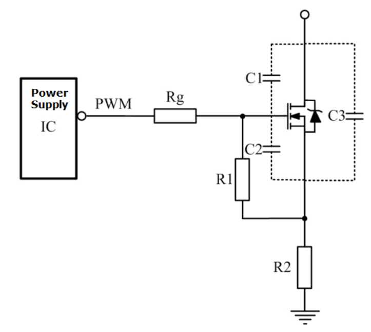
Fig. 1 IC directly drives MOS gate
Using this method, we should pay attention to several parameters and their effects.
First, check the power IC manual for the maximum peak driving current, because different IC chips have different driving capabilities.
Secondly, check the parasitic capacitance of MOSFET, such as C1, C2 and C3 in the figure. If the capacitance is large, the energy required to turn on the MOS tube is also large.
If the power IC does not have enough peak drive current, the transistor will turn on at a slower speed.If the driving capability is insufficient, high-frequency oscillation may occur at the rising edge, and even reducing Rg in Figure 1 will not solve the problem! However, IC driving ability, parasitic capacitance of MOSFET, switching speed of MOSFET and other factors will also affect the choice of driving resistance, so Rg cannot be reduced indefinitely.
2. totem pole circuit enhances driving.The function of the driving circuit is to increase the current supply capacity and quickly complete the charging process of the gate capacitor input. This topology increases the turn-on time, but reduces the turn-off time, and the switch tube can be turned on quickly, avoiding the high-frequency oscillation of the rising edge.
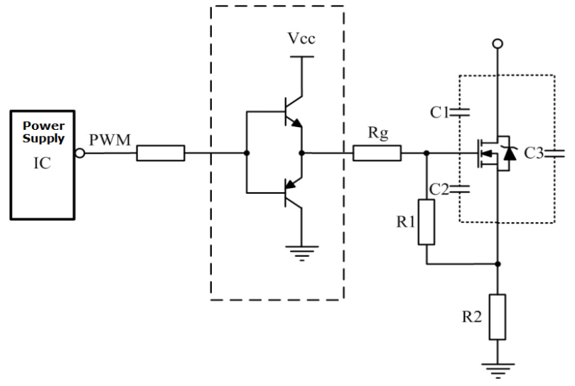 Figure 2 totem pole circuit enhanced drive
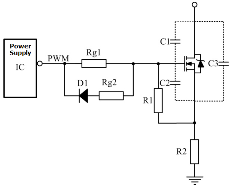 Fig. 3 accelerating MOS transistor shutdown circuit
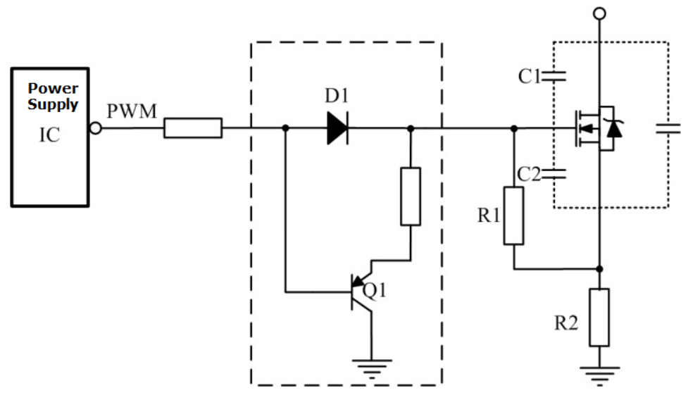 Fig. 4 improved accelerating MOS transistor shutdown circuitIt is very common to use triode to discharge the electricity of GS capacitor. If the emitter of Q1 has no resistance, the capacitor between the gate and the source of PNP transistor will be short-circuited when it is turned on, which can realize the discharge in the shortest time and minimize the cross loss when it is turned off.Fig. 4. Because of the existence of triode, the capacitor current between the gate and the source will not be discharged directly through the power IC, which improves the reliability of the circuit.

Figure 5 High-side MOSFET driver circuit
Disclaimer: This article is reproduced from "Hengli Electronics". This article only represents the author's personal views, and does not represent the views of Sacco Micro and the industry. It is only for reprinting and sharing to support the protection of intellectual property rights. Please indicate the original source and author when reprinting. If there is any infringement, please contact us to delete it.
Company Tel: +86-0755-83044319
Fax/fax:+86-0755-83975897
Email: 1615456225@qq.com
QQ: 3518641314 Manager Li
QQ: 332496225 Manager Qiu
Address: Room 809, Block C, Zhantao Technology Building, No.1079 Minzhi Avenue, Longhua New District, Shenzhen


Site Map | 萨科微 | 金航标 | Slkor | Kinghelm
RU | FR | DE | IT | ES | PT | JA | KO | AR | TR | TH | MS | VI | MG | FA | ZH-TW | HR | BG | SD| GD | SN | SM | PS | LB | KY | KU | HAW | CO | AM | UZ | TG | SU | ST | ML | KK | NY | ZU | YO | TE | TA | SO| PA| NE | MN | MI | LA | LO | KM | KN
| JW | IG | HMN | HA | EO | CEB | BS | BN | UR | HT | KA | EU | AZ | HY | YI |MK | IS | BE | CY | GA | SW | SV | AF | FA | TR | TH | MT | HU | GL | ET | NL | DA | CS | FI | EL | HI | NO | PL | RO | CA | TL | IW | LV | ID | LT | SR | SQ | SL | UK
Copyright ©2015-2025 Shenzhen Slkor Micro Semicon Co., Ltd
