Service hotline
+86 0755-83044319

release time:2022-03-17Author source:SlkorBrowse:9263
In a project, the design of PCB is only a concrete implementation process. In order to make your efforts in the past few weeks truly meaningful, the preliminary work is even more important, and more time and energy should be spent to ensure that what you do later is in the right direction.
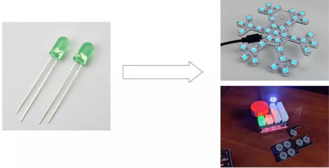
The design process of PCB is the process of turning your imagined concept into a practical and working system. Take a simple example-when the festival is coming, you want to design some cool effects with LED, and you should determine your own scheme according to your imagined scene, specific use, feasibility, cost and other factors.
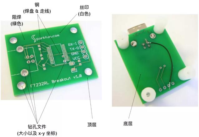
Although the ultimate goal is a printed circuit board (PCB)
However, the following process is still essential, especially for some serious products to be designed by enterprises/teams. Even if a simple idea of an individual wants to finally start your PCB design, this process is actually essential:
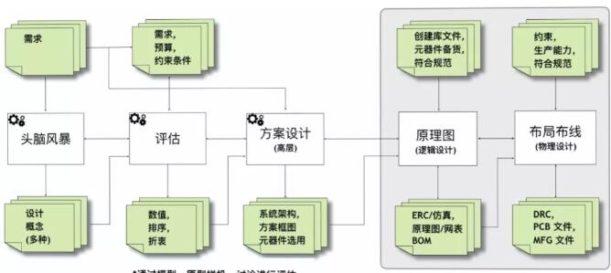
As can be seen from the above figure, the first three steps of formal PCB design (collecting ideas, comprehensive evaluation and scheme design) are very important, requiring divergent thinking and strict argumentation, borderless extension (information acquisition and reference) and precise convergence (final scheme). This process reflects the comprehensive ability of a team (or you personally) and the standardization of the process.
In the brainstorming stage, the more ideas/schemes, the better. It's best for many people to participate in the discussion and brainstorm ideas according to the needs of their own projects, but don't be constrained, especially by formal needs.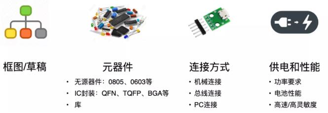
After collecting information from many parties and creative ideas, we need to converge-each idea and possibility should be analyzed for feasibility, so as to select the best scheme. Musk can launch rockets and build electric cars, but we don't have those conditions. The limited constraints make many of our beautiful ideas converge greatly. Experience, rigorous logical analysis and the collision between spear and shield are the key points at this stage:
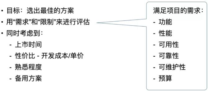
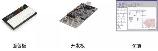
During this period, we should "confirm" some "uncertainties", and test and verify some new circuits, circuits and codes borrowed from others, so as to ensure that these "bases" are really valid. Therefore, if bread board is to be used, even an expensive development board might as well be bought. Compared with the time and opportunity cost you spent in later projects, a development board of several thousand dollars may be worth buying; You must be skilled in using some simulation software and tools for "preview". If you spend an extra hour at the moment, you may save a few months' time and save a project.
Just as the business plan is written to the entrepreneur himself, you need to form a standardized and complete product design scheme. In the form of a formal document, it must contain one or more clear scheme block diagrams+detailed analysis and argumentation of each part.
In our design, the scheme block diagram, schematic diagram and PCB board diagram represent the achievements of three key stages in product design-from the scheme block diagram, we can intuitively see the composition of the system, the connection relationship among various functional components and the signal flow. You don't need to be accurate to the pin definition of each device and the connection of each signal line between them, but it is enough to let the reader know the functions that the system can achieve, the performance indicators achieved, the possible costs, the design cycle, etc.
There is no ultimate solution in the world, even if every generation of Apple's products are not perfect, there is only a "relatively superior" solution at that time, combined with its own actual conditions and various constraints.
With this "relatively superior" scheme, we can start the PCB design.
Disclaimer: This article is reproduced from "Electronic Forest". This article only represents the author's personal views, and does not represent the views of Sacco Micro and the industry. It is only for reprinting and sharing to support the protection of intellectual property rights. Please indicate the original source and author when reprinting. If there is any infringement, please contact us to delete it.
Company Tel: +86-0755-83044319
Fax/fax:+86-0755-83975897
Email: 1615456225@qq.com
QQ: 3518641314 Manager Li
QQ: 332496225 Manager Qiu
Address: Room 809, Block C, Zhantao Technology Building, No.1079 Minzhi Avenue, Longhua New District, Shenzhen


Site Map | 萨科微 | 金航标 | Slkor | Kinghelm
RU | FR | DE | IT | ES | PT | JA | KO | AR | TR | TH | MS | VI | MG | FA | ZH-TW | HR | BG | SD| GD | SN | SM | PS | LB | KY | KU | HAW | CO | AM | UZ | TG | SU | ST | ML | KK | NY | ZU | YO | TE | TA | SO| PA| NE | MN | MI | LA | LO | KM | KN
| JW | IG | HMN | HA | EO | CEB | BS | BN | UR | HT | KA | EU | AZ | HY | YI |MK | IS | BE | CY | GA | SW | SV | AF | FA | TR | TH | MT | HU | GL | ET | NL | DA | CS | FI | EL | HI | NO | PL | RO | CA | TL | IW | LV | ID | LT | SR | SQ | SL | UK
Copyright ©2015-2025 Shenzhen Slkor Micro Semicon Co., Ltd
