Service hotline
+86 0755-83044319

release time:2024-03-13Author source:SlkorBrowse:2730
MOSFET, field effect transistor (MOSFET), is a kind of voltage-controlled power switching element, which is widely used in switching power supply, inverter, DC motor driver and other devices, and is the core component of power electronics.
MOSFET are divided into N-channel and P-channel, and N-channel is equivalent to NPN triode; P channel is equivalent to PNP triode. In actual design and application, the N-channel MOSFET accounts for the vast majority, so the following explanation is given by taking the N-channel MOSFET as an example (as shown in Q3, gate-G in Figure 1; Drain-d; Source -S).The use of MOSFET can usually be divided into two situations:① Participate in common logic control, and use it as a switching tube like a triode, with a current of several amperes. As shown in Figure 1, the MOSFETdrives the DC motor circuit. R6 pull-down resistor is necessary (the value is generally 10--20k), and its principle is the same as that of NPN triode pull-down resistor.The Vgs voltage of MOSFET in this kind of application is 4.5V higher than the threshold voltage (also called platform voltage), so it can be used normally. I still choose to use triode for low-power logic control.
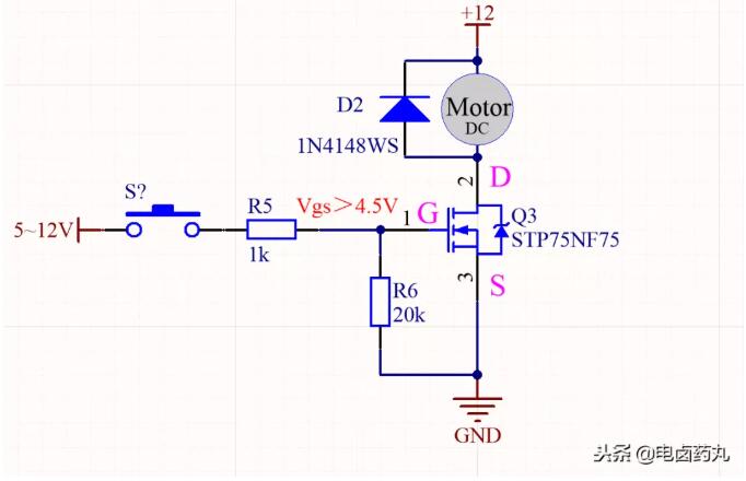
Figure 1: Logic Control MOSFET
② Participation in PWM control, bridge drive circuit and switching power supply circuit are widely used.Figure 2 shows the bridge drive circuit of the brush DC motor. G1, G2, G3 and G4 are controlled by push-pull PWM, and VS1 and VS2 are connected to the motor, which can realize the speed regulation and forward and reverse control of the high-power DC motor. The Vgs voltage of MOSFET in this kind of application is greater than 10V, and usually 12V is used (to ensure the conduction depth, the amplitude of PWM is 12V). And the resistance of the G pole must be small, usually 4.7-100Ω, and a reverse diode is connected in parallel with the resistance, so as to ensure that the turn-off speed of the MOSFET is faster than the turn-on speed and prevent the upper bridge and the lower bridge from being directly short-circuited.
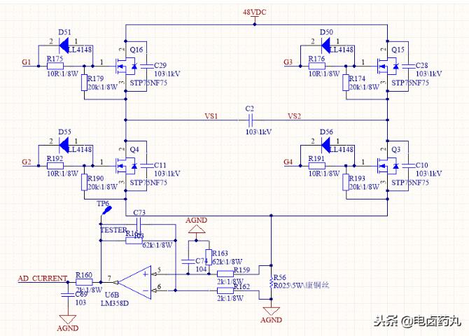
Figure 2:
Bridge Drive Circuit of Brushed DC MotorTo thoroughly understand MOSFET, we should start with the following two points:① What is Miller effect and why there is Vgs platform voltage under Miller effect;
② Switching loss, conduction loss and freewheeling loss of ②MOSFET.
As shown in Figure 3, there is an inter-electrode capacitance Cgd between G and D, and an inter-electrode capacitance Cgs between G and S. When there is a high-level signal at G, when the capacitance Cgs charges to the threshold voltage of 4.5V, the DS begins to conduct, and the D-pole level drops to 0V. During this process, the capacitance Cgd starts to charge, keeping the G-pole voltage at 4.5V in a short time, which is the Miller effect.
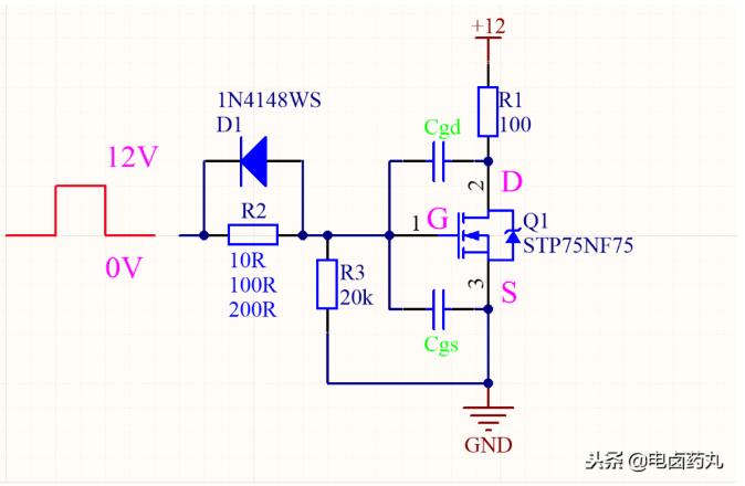
Figure 3: Schematic diagram of Miller effect test
The threshold voltage Vgs is the platform voltage of MOS transistor; The platform voltage exists during the turn-on and turn-off of MOS transistor, and its width is directly related to the resistance of G electrode.
Fig. 4 shows the waveform of MOS transistor when G-pole resistance is 10Ω. Red represents the voltage waveform of Vgs and blue represents the voltage waveform of Vds. The width of the platform voltage is very narrow (yellow arrow). Under the platform voltage, there is a varistor area between DS poles, and Vds is very narrow (green arrow).
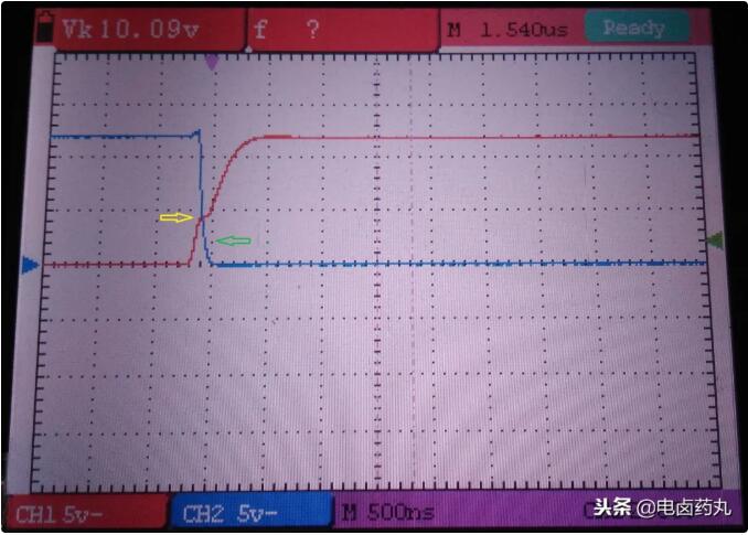
Figure 4: G-pole resistance is 10Ω, Vgs and Vds waveforms (on)
As shown in Figure 5, when the resistance of G pole is 100Ω, the MOS transistor is turned on, and the width of the platform voltage is obviously widened (yellow arrow). Under the platform voltage, there is a variable resistance area between DS poles, and the Vds becomes slow (green arrow).
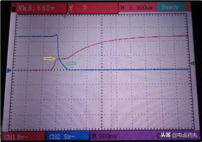
Figure 5: G-pole resistance is 100Ω, Vgs and Vds waveforms (on)
As shown in Figure 6, when the resistance of G pole is 200Ω, the MOS transistor turns on, and the width of the platform voltage becomes wider (yellow arrow). Under the platform voltage, there is a variable resistance area between DS poles, and the Vds becomes slower and slower (green arrow).
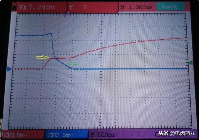
Figure 6: G-pole resistance is 200Ω, Vgs and Vds waveforms (on) Figure 7 shows the waveform of the MOS transistor when the G-pole resistance is 200Ω, and there is also the platform voltage.
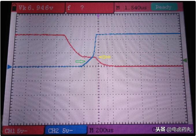
Figure 7: VGS and Vds waveforms (off)The loss of MOSFET means heating.
To make MOSFET work normally, we must know all kinds of losses.
As shown in Figure 8:The switching loss is divided into the turning-on loss and the turning-off loss of MOS transistor. The G-pole resistance determines the turning-on and turning-off speed, and the larger the resistance, the greater the switching loss.
The conduction loss depends on the equivalent resistance Rds(on) between DS poles, and the greater the resistance, the greater the conduction loss.The freewheeling loss refers to the loss of the forward diode between the S pole and the D pole, which is usually not considered (omitted in this article).
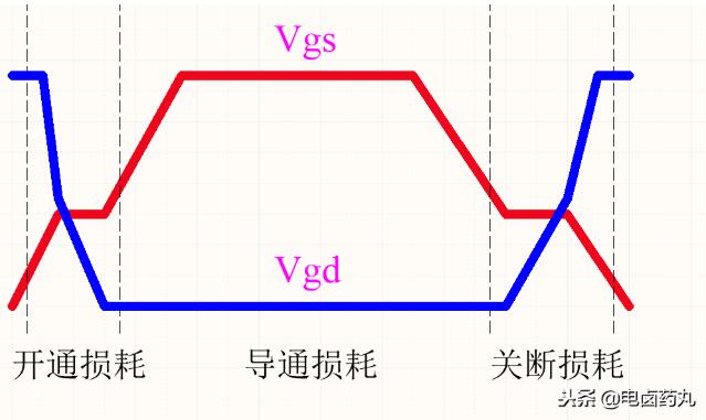
Figure 8: Main losses of 8:MOSFET
As shown in Figure 9, for the selection of MOSFET, the main parameters will be given directly in front (in the red box), and DS pole withstand voltage (Vdss) is usually 1.5-2 times of the working voltage; The drain current (Id) is usually 5-10 times of the working current; Rds(on) should be as small as possible. In addition, the Vgs voltage range of the g pole is ± Within 20V, almost all MOSFET are like this.
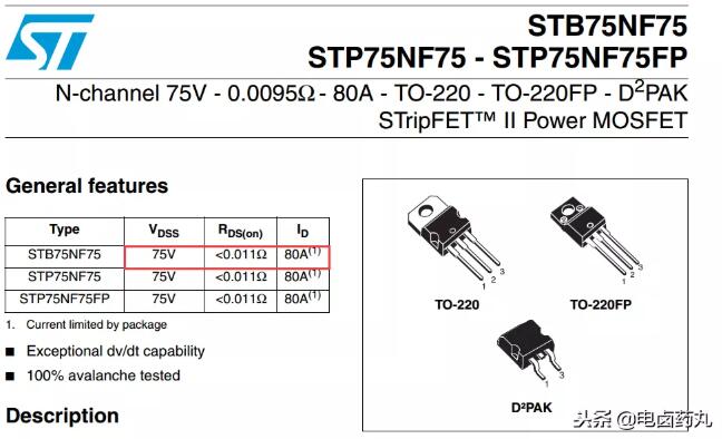
Figure 9: MOSFET parameters
Therefore, the switching loss of MOS transistor is directly related to the design, and shortening the on-off time can effectively reduce the switching loss. Finally, many push-pull circuits for driving MOS transistors have been integrated in the driving chip, and the output capacity is very strong, usually the current can reach 1A.


Site Map | 萨科微 | 金航标 | Slkor | Kinghelm
RU | FR | DE | IT | ES | PT | JA | KO | AR | TR | TH | MS | VI | MG | FA | ZH-TW | HR | BG | SD| GD | SN | SM | PS | LB | KY | KU | HAW | CO | AM | UZ | TG | SU | ST | ML | KK | NY | ZU | YO | TE | TA | SO| PA| NE | MN | MI | LA | LO | KM | KN
| JW | IG | HMN | HA | EO | CEB | BS | BN | UR | HT | KA | EU | AZ | HY | YI |MK | IS | BE | CY | GA | SW | SV | AF | FA | TR | TH | MT | HU | GL | ET | NL | DA | CS | FI | EL | HI | NO | PL | RO | CA | TL | IW | LV | ID | LT | SR | SQ | SL | UK
Copyright ©2015-2022 Shenzhen Slkor Micro Semicon Co., Ltd
