Service hotline
+86 0755-83044319
release time:2022-04-01Author source:slkorBrowse:8117
Main internal losses of switching power supply To improve the efficiency of switching power supply, it is necessary to distinguish and roughly estimate various losses. The internal loss of switching power supply can be roughly divided into four aspects: switching loss, conduction loss, additional loss and resistance loss. These losses usually occur simultaneously in lossy components, which will be discussed separately below.Main internal losses of switching power supply To improve the efficiency of switching power supply, it is necessary to distinguish and roughly estimate various losses. The internal loss of switching power supply can be roughly divided into four aspects: switching loss, conduction loss, additional loss and resistance loss. These losses usually occur simultaneously in lossy components, which will be discussed separately below.
Losses associated with power switches
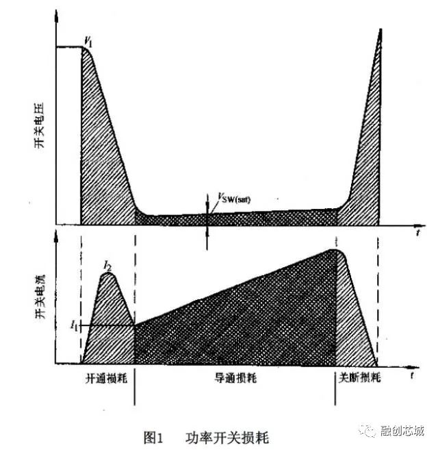
Power switch is one of the two main loss sources in a typical switching power supply. Loss can be basically divided into two parts: conduction loss and switching loss. The conduction loss is the loss when the power switch is in the conduction state after the power device has been turned on and the driving and switching waveforms have stabilized. Switching loss is the loss that occurs when the power switch is driven into a new working state and the driving and switching waveforms are in the transition process. These stages and their waveforms are shown in Figure 1.
The conduction loss can be measured by the product of voltage and current waveforms across the switch. These waveforms are all approximately linear, and the power loss during conduction is given by Formula (1).

The typical way to control this loss is to minimize the voltage drop during the conduction of the power switch. To achieve this goal, the designer must make the switch work in saturation. These conditions are given by Formula (2a) and Formula (2b). Through base or gate overcurrent driving, it is ensured that the collector or drain current is controlled by external components instead of the power switch itself.

The switching loss during power switching is more complicated, which has its own factors and the influence of related components. The waveform related to the loss can only be observed by an oscilloscope with a voltage probe connected to the drain-source (collector-emitter) terminal, and an AC current probe can measure the drain or collector current. When measuring the instantaneous loss of each switch, a shielded short-lead probe must be used, because any unshielded wire with a length may introduce noise from other power sources, and thus the true waveform cannot be accurately displayed. Once a good waveform is obtained, the area enclosed by these two curves can be roughly calculated by simple triangle and rectangle subsection summation method. For example, the turn-on loss of fig. 1 can be calculated by equation (3).

This result is only the loss value of the power switch during the on period, and the total loss value during the on period can be obtained by adding the off and on losses.
Losses associated with output rectifier
In the total internal loss of typical asynchronous rectifier switching power supply, the loss of output rectifier accounts for 40%-65% of the total loss. So it is very important to understand this section. The waveforms related to the output rectifier can be seen in Figure 2.
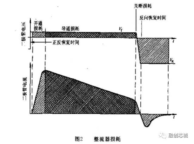
Rectifier loss can also be divided into three parts: turn-on loss, turn-on loss and turn-off loss.
The conduction loss of the rectifier is the loss when the rectifier is conducting and the current and voltage waveforms are stable. This loss is suppressed by selecting the rectifier with the lowest forward voltage drop when a certain current flows. PN diode has flatter forward V-I characteristic, but its voltage drop is higher (0.7 ~ 1.1V). Schottky diode has a low turning voltage (0.3 ~ 0.6V), but its voltage-current characteristic is not too steep, which means that with the increase of current, its direct voltage increases faster than that of PN diode. The transition process in the waveform is segmented into rectangular and triangular areas, and this loss can be calculated by formula (3).
It is much more complicated to analyze the switching loss of the output rectifier. The inherent characteristics of rectifier will cause many problems in local circuits.
During the opening period, the transition process is determined by the positive recovery characteristics of the rectifier tube. The recovery time tfrr is the time from the time when the direct voltage is applied across the diode to the time when the forward current begins to flow. For PN fast recovery diode, this time is 5 ~ 15 ns. Schottky diodes sometimes exhibit longer forward recovery time due to their inherent higher junction capacitance. Although this loss is not very big, it can cause other problems inside the power supply. During the recovery period, the inductor and transformer have no large load impedance, while the power switch or rectifier is still in the off state, which makes the stored energy oscillate until the rectifier finally starts to flow forward current and clamp the power signal.
At the turn-off moment, the reverse recovery characteristic plays a major role. When the reverse voltage is applied across the diode, the reverse recovery characteristic of PN diode is determined by the carriers in the junction. These carriers with limited mobility need to go out from the opposite direction that they originally entered the junction, thus constituting the reverse current flowing through the diode. The loss associated with this may be great, because before the junction charge is exhausted, the reverse voltage will rise rapidly, and the reverse current will be reflected to the primary power switch through the transformer, which will increase the loss of the power tube. Take Figure 1 as an example, you can see the peak current during the turn-on period.
Similar reverse recovery characteristics will also appear in high-voltage Schottky rectifiers. This characteristic is not caused by carriers, but by the high junction capacitance of these Schottky diodes. The so-called high-voltage Schottky diode means that its reverse breakdown voltage is greater than 60V.Similar reverse recovery characteristics will also appear in high-voltage Schottky rectifiers. This characteristic is not caused by carriers, but by the high junction capacitance of these Schottky diodes. The so-called high-voltage Schottky diode means that its reverse breakdown voltage is greater than 60V.
Losses related to filter capacitance
Input filter capacitors are not the main loss source of switching power supply, although they have great influence on the working life of power supply. If the input capacitor is not selected correctly, the power supply can't achieve its actual high efficiency.Input filter capacitors are not the main loss source of switching power supply, although they have great influence on the working life of power supply. If the input capacitor is not selected correctly, the power supply can't achieve its actual high efficiency.
Each capacitor has a small resistance and inductance in series with the capacitor. The equivalent series resistance (ESR) and the equivalent series inductance (ESL) are parasitic elements caused by the structure of the capacitor, and they both hinder the external signal from being applied to the internal capacitor. Therefore, the capacitor has the best performance when working in DC, but its performance will be much worse at the switching frequency of the power supply.
The input capacitor is the only source (or storage place) of high-frequency current generated by power switch or output rectifier, so the current flowing through ESR of these capacitors can be reasonably determined by observing these current waveforms. This current inevitably generates heat in the capacitor. The main task of designing the filter capacitor is to ensure that the internal heat of the capacitor is low enough to ensure the life of the product. Equation (4) gives the calculation formula of power loss caused by ESR of capacitor.

Not only the resistance part of the capacitor model will cause problems, but also if the lead wires of parallel capacitors are asymmetric, the lead wire inductance will make the internal heating of the capacitor unbalanced, thus shortening the life of the capacitor with the highest temperature.
supplementary loss
The additional loss is related to all the functional devices required to run the power circuit, including the circuits related to the control IC and the feedback circuits. Compared with other losses of power supply, these losses are generally small, but some analysis can be made to see if there is any possibility of improvement.The additional loss is related to all the functional devices required to run the power circuit, including the circuits related to the control IC and the feedback circuits. Compared with other losses of power supply, these losses are generally small, but some analysis can be made to see if there is any possibility of improvement.
First, start the circuit. The starting circuit obtains DC current from the input voltage, so that the control IC and the driving circuit have enough energy to start the power supply. If this startup circuit can't cut off the current after the power is started, the circuit will have a continuous loss of up to 3W, and the loss depends on the input voltage.
The second main aspect is the power switch driving circuit. If a bipolar power transistor is used for the power switch, the base drive current must be greater than the peak current of the collector E of the transistor divided by the gain (hFE). The typical gain of the power transistor is between 5 and 15, which means that if it is a peak current of 10A, it requires a base current of 0.66 ~ 2A. There is a voltage drop of 0.7V between the base and emitter. If the base current is not obtained from a voltage very close to 0.7V, a great loss will occur.
The driving efficiency of power MOSFET is higher than that of bipolar power transistor. The gate of MOSFET has two equivalent capacitors connected to the drain and source, namely gate-source capacitor Ciss and drain-source capacitor Crss. The loss of gate drive of MOSFET comes from the charging of gate capacitor by auxiliary voltage when MOSFET is turned on, and discharging to ground when MOSFET is turned off. The calculation of gate loss is given by Equation (5).

For this loss, there is not much to be done except to select MOSFET with lower Ciss and Crss values, so that it is possible to slightly reduce the maximum gate driving voltage.
Losses associated with magnetic elements
For general design engineers, this part is very complicated. Because of the particularity of magnetic element terminology, the following losses are mainly represented by the magnetic core manufacturers in the form of charts, which is very convenient to use. These losses are listed here, so that people can evaluate the nature of the losses.
There are three main losses related to transformers and inductors: hysteresis loss, eddy current loss and resistance loss. These losses can be controlled when designing and constructing transformers and inductors.
Hysteresis loss is related to the number of turns of winding and driving mode. It determines the area swept in the B-H curve in each working cycle. The swept area is the work done by the magnetic field force, which rearranges the magnetic domains in the magnetic core. The larger the swept area, the greater the hysteresis loss. The loss is given by equation (6).

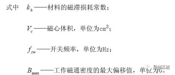
As can be seen from the formula, the loss is proportional to the quadratic of the working frequency and the maximum working magnetic flux density. Although this loss is not as big as the loss inside the power switch and rectifier, improper treatment will also become a problem. At 100kHz, Bmax should be set to 50% of the saturation magnetic flux density Bsat of the material. At 500kHz, Bmax should be set to 25% of the saturation magnetic flux density Bsat of the material. At 1MHz, Bmax should be set to 10% of the material saturation magnetic flux density Bsat. This is determined by the characteristics of ferromagnetic materials in switching power supplies (3C8, etc.).
Eddy current loss is much smaller than hysteresis loss, but it increases rapidly with the increase of operating frequency, as shown in equation (7).


Eddy current is a circulating current induced in a large range inside the magnetic core in a strong magnetic field. Generally, designers don't have many ways to reduce this loss.Eddy current is a circulating current induced in a large range inside the magnetic core in a strong magnetic field. Generally, designers don't have many ways to reduce this loss.
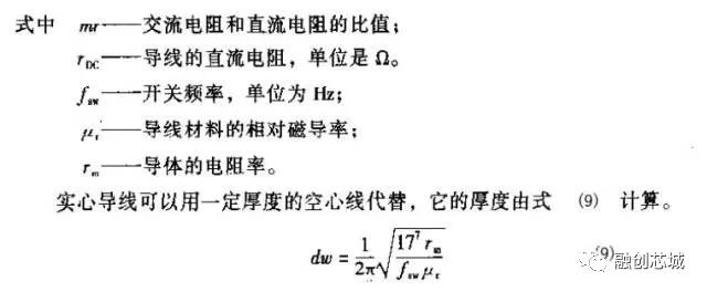
Resistance loss is the loss caused by the resistance of the internal winding of transformer or inductor. There are two forms of resistance loss: DC resistance loss and skin effect resistance loss. The DC resistance loss is determined by the product of the resistance of the winding wire and the square of the effective value of the current flowing through it. The skin effect is caused by the strong AC electromagnetic field in the conductor, and the current in the center of the conductor is pushed to the surface of the conductor, which actually increases the resistance of the conductor. The current flows in a smaller section, which makes the effective diameter of the conductor appear smaller. Equation (8) gives the calculation formula of these two losses in one expression.

Leakage inductance (represented by a small inductance connected in series with the winding) makes a part of magnetic flux leak into the surrounding air and materials without interlocking with the magnetic core. Its characteristics are not affected by its associated transformer or inductance, so the reflection impedance of the winding does not affect the performance of leakage inductance.
Leakage will cause a problem because it does not transmit power to the load, but generates oscillating energy in the surrounding elements. In the structural design of transformer and inductor, the leakage inductance of winding should be controlled. The leakage inductance value of each one will be different, but it can be controlled to a certain rated value.
Some general rules of thumb to reduce winding leakage inductance are: lengthening the length of winding, getting closer to the magnetic core, tight coupling technology between windings, and similar turns ratio (such as close to L: 1). For the E-E core commonly used in DC-DC converters, the estimated leakage inductance is 3% ~ 5% of the winding inductance. In an off-line converter, the leakage inductance of the primary winding may be as high as 12% of the winding inductance, if the transformer has to meet strict safety regulations. The tape used to insulate the winding will make the winding shorter and keep it away from the magnetic core and other windings.
It can be seen later that the additional loss caused by leakage inductance can be utilized.
In the application of DC magnet, there is usually an air gap along the magnetic circuit of the magnetic core. In a ferrite core, the air gap is in the middle of the core, and the magnetic flux flows from one end of the core to the other, although the magnetic lines will spread out from the center of the core. The existence of air gap creates a dense magnetic flux area, which will cause eddy current flow in the metal parts near the coil or air gap. This loss is generally not great, but it is difficult to determine.
Overview of Main Parasitic Parameters in Power Supply
Parasitic parameters are unexpected electrical characteristics of the actual components inside the circuit. They generally store energy and react on their own components to produce noise and loss. It is a great challenge for designers to distinguish, quantify, reduce or make use of these adverse reactions.
In the case of communication, the parasitic characteristics are more obvious. There are two main nodes with large AC value in a typical switching power supply, the first is the collector or drain of the power switch; The second is the anode of the output rectifier. We must focus on these two special nodes.
Main parasitic parameters in converter
In all switching power supplies, there are some common parasitic parameters, and their influence can be clearly seen when observing the waveforms of the main AC nodes in the converter. Some data of devices even give these parameters, such as parasitic capacitance of MOSFET. The main parasitic parameters of two common converters are shown in Figure 3.
Some parasitic parameters have been clearly defined, such as the capacitance of MOSFET, while other discrete parasitic parameters can be expressed by lumped parameters, which makes modeling easier. It is very difficult to determine the values of parasitic parameters that are not clearly defined, and they are usually determined by an empirical value. In other words, when designing soft switches, the selection of components should be based on the principle of getting the best results. In the circuit diagram, it is very important to place parasitic elements in proper places, because the electrical branch only works for a part of the converter's working time. For example, the junction capacitance of the rectifier will be large only when the rectifier is biased in the reverse direction, but will disappear when the diode is biased in the forward direction. Table L lists some parasitic parameters that are easy to determine, the components that generate these parameters, and the approximate range of these values. Some special parasitic parameter values can be obtained from the data of specific components.
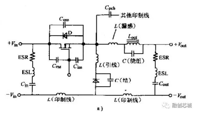
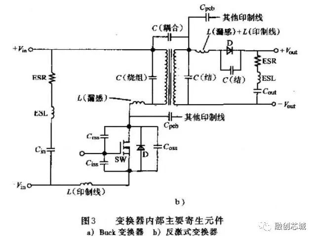
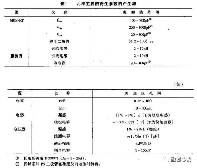
The influence of printed circuit board (PCB) on parasitic parameters is everywhere, and good PCB layout rules can minimize these influences.
Printed lines with peak current are sensitive to inductance and capacitance generated by any printed line, so these lines must be short and thick. PCB solder joints with AC high voltage, such as drain or collector of power switch or anode of rectifier tube, are easy to generate coupling capacitance with adjacent printed lines, so that AC noise is coupled into adjacent printed lines. Through the "via" connection, the same signal can flow through the upper and lower layers of the AC signal printed circuit. The influence of other parasitic parameters can generally be attributed to adjacent parasitic elements.
Knowing the nature of parasitic parameters on each component of a typical converter will help to determine the parameters of magnetic components, design PCB, design EMI filter, etc. This is the most difficult part of all switching power supply designs.


Site Map | 萨科微 | 金航标 | Slkor | Kinghelm
RU | FR | DE | IT | ES | PT | JA | KO | AR | TR | TH | MS | VI | MG | FA | ZH-TW | HR | BG | SD| GD | SN | SM | PS | LB | KY | KU | HAW | CO | AM | UZ | TG | SU | ST | ML | KK | NY | ZU | YO | TE | TA | SO| PA| NE | MN | MI | LA | LO | KM | KN
| JW | IG | HMN | HA | EO | CEB | BS | BN | UR | HT | KA | EU | AZ | HY | YI |MK | IS | BE | CY | GA | SW | SV | AF | FA | TR | TH | MT | HU | GL | ET | NL | DA | CS | FI | EL | HI | NO | PL | RO | CA | TL | IW | LV | ID | LT | SR | SQ | SL | UK
Copyright ©2015-2025 Shenzhen Slkor Micro Semicon Co., Ltd