Service hotline
+86 0755-83044319

release time:2025-05-12Author source:SlkorBrowse:6124
In cutting-edge technologies such as 5G communication, millimeter-wave radar, and high-speed serial buses, signal integrity has become a key factor in determining system performance. As the "invisible guardian" of circuit protection, the evolution of Electrostatic Discharge (ESD) protection diodes is transitioning from purely functional protection to high-frequency performance optimization. This article will explore how the breakthrough parameter design of the GBLC05CI ESD protection diode from a certain brand is reshaping the protection architecture of high-frequency electronic systems.
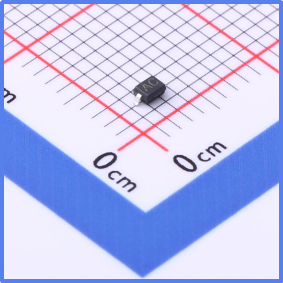
Slkor Electrostatic Discharge Diode GBLC05CI product photo
The GBLC05CI is a new-generation ultra-low capacitance ESD protection device designed for 5V power supply systems. It comes in an SOD-323 package (size: 2.5×1.3×1.1mm), and its core target markets include:
5G base station RF front-end modules
High-speed serial interfaces above 10Gbps (e.g., USB 3.2 Gen2×2, PCIe 4.0)
Automotive Ethernet (1000BASE-T1/10GBASE-T1)
Millimeter-wave radar antenna ports
High-end consumer electronics HDMI 2.1 interfaces
Its technological breakthrough lies in two key dimensions: the unified solution of a 0.8pF industry-leading junction capacitance and an 18V low clamping voltage. This achieves both GHz-level signal transmission requirements and surge protection capabilities that surpass traditional devices.

Slkor Electrostatic Discharge Diode GBLC05CI specification

Parameters of Slkor Electrostatic Discharge Diode GBLC05CI
1. Reverse Working Voltage (VRWM=5V ±5%)
This parameter is precisely matched to the 5V operating voltage of digital circuits, ensuring that over a full temperature range of -55°C to +175°C, the device's leakage current (Ir=1μA) has negligible impact on system power consumption. The ±5% tolerance control is superior to the industry average (±10%) and effectively prevents false triggering risks caused by power fluctuations.
2. Breakdown Voltage (VBR min=6V)
When the ESD pulse voltage exceeds 6V, the device enters avalanche breakdown and conducts. This design provides dual protection:
Protection Delay Optimization: The device enters protection mode 25% earlier than traditional devices (VBR min=8V).
Improved Immunity: It prevents malfunction caused by noise, especially in industrial environments.
3. Clamping Voltage (VC=18V@IPP=3A)
Under the 8/20μs standard test waveform, when the surge current reaches 3A, the device limits the voltage to 18V. Compared to similar devices (VC≈25V), its advantages include:
A wider safety margin for 5V-powered 1.8V/3.3V CMOS devices.
A 60% reduction in dynamic resistance (Rdyn=6Ω), offering more efficient clamping.
4. Junction Capacitance (Cj=0.8pF@1MHz)
Through three-dimensional ion implantation and dielectric layer optimization, the junction capacitance is reduced by 95% compared to traditional devices (15pF), achieving:
Insertion loss (S21) < 0.2dB at 10GHz, with a 40% improvement in eye diagram margin.
Phase noise (at 1MHz offset) improved by 15dBc, meeting the phase-sensitive requirements of radar systems.
5. High-Speed Response Characteristics
Response Time (tr/tf < 500ps): Uses step-doping profile design for sub-nanosecond-level response.
Parasitic Inductance (Lstray < 0.5nH): Through optimized lead packaging, it reduces high-frequency oscillation risks.
1. 5G Millimeter-Wave Front-End Protection
In the 28GHz band, the 0.8pF capacitance results in only 0.03dB signal attenuation, which can be placed in parallel between the antenna switch and power amplifier. Design considerations include:
Ground vias with a diameter ≥0.2mm to reduce parasitic inductance.
Using coplanar waveguide (CPW) layout, with a characteristic impedance of 50Ω.
Device spacing >3mm to avoid thermal coupling.
2. 10Gbps High-Speed Interfaces
For USB 3.2 Gen2×2 (20Gbps) applications, a differential pair layout is recommended:
One GBLC05CI in parallel with each channel, with isolation between channels >40dB at 10GHz.
Verified through eye diagram testing, jitter increase <2ps.
Insertion loss meets IEEE 802.3bj specification requirements.
3. Automotive Ethernet Protection
In 1000BASE-T1 applications, considerations include:
Coordination between common-mode chokes and ESD devices.
Meeting AEC-Q101 automotive-grade reliability standards.
Capacitance variation rate <5% over the temperature range of -40°C to +125°C.
4. Performance Advantages and Industry Evolution
Compared to traditional ESD protection solutions, the GBLC05CI offers three major technological advantages:
1. Signal Integrity Revolution: The 0.8pF junction capacitance breakthrough enables data rates to jump from the Gbps to 10Gbps+ range.
2. Increased Protection Density: The SOD-323 package is 60% smaller than the SOT-23, making it ideal for high-density PCB layouts.
3. System Cost Optimization: A single device can replace the "TVS + filter" combination, reducing BOM costs by about 25%.
Currently, ESD protection devices are experiencing two major development trends:
Material Innovation: Gallium nitride (GaN)-based ESD devices are entering the research and development stage, aiming for THz-band protection.
Function Integration: Multi-functional devices integrating ESD protection and EMI filtering are beginning mass production.
The GBLC05CI ESD protection diode, with its optimized parameters, provides a new protection solution for high-frequency electronic systems. Its design philosophy reveals the direction of industry evolution: at the nanometer process node, ESD devices have evolved from passive protection components to core components actively participating in system design. For engineers, deeply understanding the mapping relationship between device parameters and system requirements will be key to achieving high performance and reliability in products. With the ongoing development of 5G and AIoT technologies, innovative devices like the GBLC05CI are redefining the boundaries of electronic system protection.
Slkor has research and development offices in Busan, South Korea, Beijing, China, and Suzhou, China. Most of the wafer manufacturing and packaging and testing are carried out within China. The company employs and collaborates with individuals and organizations worldwide, with a laboratory for product performance and reliability testing and a central warehouse located at its headquarters in Shenzhen. Slkor has filed for over a hundred invention patents, offers more than 2,000 product models, and serves over ten thousand customers globally. Its products are exported to countries and regions including Europe, the Americas, Southeast Asia, and the Middle East, making it one of the rapidly growing semiconductor companies in recent years. With well-established management systems and streamlined workflows, Slkor has rapidly enhanced the brand awareness and reputation of its "SLKOR" brand through its outstanding quality and standardized services. Its product range includes three major series: diodes, transistors, and power devices, with recent introductions of new products such as Hall elements and analog devices, expanding its presence in sensors, Risc-v microcontrollers, and other product categories.


Site Map | 萨科微 | 金航标 | Slkor | Kinghelm
RU | FR | DE | IT | ES | PT | JA | KO | AR | TR | TH | MS | VI | MG | FA | ZH-TW | HR | BG | SD| GD | SN | SM | PS | LB | KY | KU | HAW | CO | AM | UZ | TG | SU | ST | ML | KK | NY | ZU | YO | TE | TA | SO| PA| NE | MN | MI | LA | LO | KM | KN
| JW | IG | HMN | HA | EO | CEB | BS | BN | UR | HT | KA | EU | AZ | HY | YI |MK | IS | BE | CY | GA | SW | SV | AF | FA | TR | TH | MT | HU | GL | ET | NL | DA | CS | FI | EL | HI | NO | PL | RO | CA | TL | IW | LV | ID | LT | SR | SQ | SL | UK
Copyright ©2015-2025 Shenzhen Slkor Micro Semicon Co., Ltd
