Service hotline
+86 0755-83044319

release time:2025-05-09Author source:SlkorBrowse:5678
With the rapid development of portable devices and IoT terminals, ESD (Electrostatic Discharge) protection components face dual challenges: they must withstand transient high-voltage surges while fitting into extremely compact circuit layouts. The SLESD5Z7V0 ESD protection diode stands out with its unique parameter combination, offering precise protection in low-voltage applications. This article will explore its technical parameters and explain how its optimized design achieves a balance between low power consumption, compact size, and reliable protection.
1. VRWM=7V: The Ideal Gatekeeper for Low-Voltage Systems
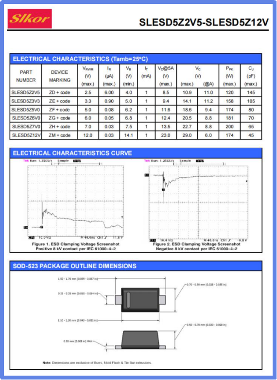
VRWM (Reverse Working Voltage) defines the safe voltage threshold for the device during normal operation. The 7V rating of the SLESD5Z7V0 is well-suited for digital circuits powered by 3.3V/5V, such as Bluetooth chips, MCU I/O ports, and sensor interfaces. When the circuit voltage is below 7V, the diode remains in a high-resistance state with a reverse leakage current (IR) as low as 0.03μA, making the static power consumption virtually negligible and significantly extending battery life.
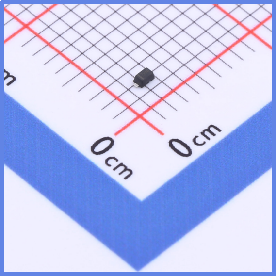
Slkor Electrostatic Discharge Diode SLESD5Z7V0 product photo
2. VBR min=7.5V: Precise Control of Breakdown Voltage
VBR (Breakdown Voltage) is the critical point where the device transitions from cutoff to conduction. The minimum breakdown voltage of 7.5V (with a typical value that may be higher) ensures the device will not mistakenly trigger during power fluctuations or transient over-voltage events. For example, in a 5V system, the 7.5V breakdown voltage helps prevent false triggering due to power ripple, while providing a quick response path for ESD pulses.
Slkor Electrostatic Discharge Diode SLESD5Z7V0 specification
3. VC=13.5V: The Safe Boundaries of Clamping Voltage
Clamping voltage (VC) refers to the device's ability to limit voltage to a safe range during an ESD event. Under IEC 61000-4-2 testing (±8kV contact discharge), the SLESD5Z7V0 clamps transient voltage within 13.5V. For digital chips with a 5V rating, this 13.5V clamping voltage provides an 8.5V safety margin, far exceeding the energy levels of typical ESD events and ensuring downstream circuits are protected from high-voltage surges.
Parameters of Slkor Electrostatic Discharge Diode SLESD5Z7V0
4. CJ=65pF: Tailored Design for Junction Capacitance
The 65pF junction capacitance (CJ) indicates that the device is optimized for low-speed signals or power lines. In low to mid-speed interfaces like USB 2.0 (480Mbps) or I2C (1Mbps), the impact of the 65pF capacitance on signal integrity can be compensated through circuit design, while its effect on system performance is almost negligible in power lines or button scanning circuits. This design choice highlights the device's targeted optimization for specific application scenarios.
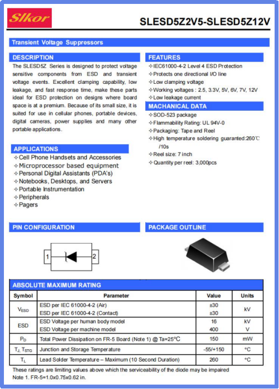
5. SOD-523 Package: The Ultimate Breakthrough in Space Efficiency
The SOD-523 package (1.0mm×0.6mm) is just one-third the size of the SOD-323 package but can withstand 8kV ESD surges (IEC standard). Its ultra-compact design allows it to be mounted on pads with a 0.4mm pitch, making it ideal for extremely space-constrained environments such as smartwatches and TWS earbud motherboards, while also compatible with high-precision automated placement processes.
1. Ultra-Low Leakage Current and Power Consumption Optimization
The 0.03μA reverse leakage current is achieved through optimized PN junction doping concentration and surface passivation. Within a wide temperature range of -55℃ to 150℃, IR fluctuation is controlled within ±10%, preventing DC offset or increased battery self-discharge due to temperature changes. This feature is crucial for the long-term reliability of wearable devices.
2. Dynamic Response and Thermal Management
Despite its compact package, the SLESD5Z7V0 uses an improved TVS structure with a response time of less than 1ns, enabling it to quickly discharge ESD currents. Its thermal resistance (θJA) is optimized to 400℃/W through three-dimensional stacked chip technology, ensuring that the junction temperature increases by only about 20℃ under a single 8kV ESD surge, meeting AEC-Q101 automotive-grade reliability requirements.
3. Balancing Clamping Voltage and Power Dissipation
The 13.5V clamping voltage, combined with the 65pF capacitance, gives the device a low impedance characteristic (typical value of 0.3Ω) during ESD events. By optimizing doping concentration and metalization layer thickness, the device can dissipate pulse power up to 500W (8/20μs), which is sufficient to handle most ESD threats in consumer electronics applications.
1. Portable Device Power Management
In battery management circuits for smartphones and tablets, the SLESD5Z7V0 can protect power lines of charging interfaces (such as USB-C). Its 7V VRWM and 13.5V clamping voltage are well-suited for 5V/9V fast charging protocols, while the 65pF capacitance has no negative impact on power ripple suppression.
2. IoT Sensor Interfaces
For low-speed analog signal interfaces like temperature and humidity sensors or accelerometers, the 65pF junction capacitance has minimal impact on signal bandwidth, which can be further reduced by layout optimization (e.g., shortening trace lengths). The 7.5V breakdown voltage effectively protects against human electrostatic discharge (typically ≤8kV).
3. Wearable Device Button Scanning
In the button circuits of smart bands and wireless earphones, the SOD-523 package can be mounted near FPC connectors. Its 0.03μA leakage current prevents additional power consumption when buttons are in sleep mode, while the 13.5V clamping voltage protects against human electrostatic discharge.
Through precise parameter tuning, the SLESD5Z7V0 paves the way for low-voltage, low-power applications in the field of ESD protection. Its 7V operating voltage suits mainstream portable devices, the 13.5V clamping voltage provides ample safety margin, the 65pF capacitance balances performance and cost, and the SOD-523 package sets a new standard for space efficiency. Its design philosophy reveals the evolutionary direction of modern electronic protection devices—optimizing electrical, thermal, and mechanical performance at the micro scale. As 5G, IoT, and wearable devices become more widespread, such "small yet precise" components will be a key foundation for ensuring system stability.
Slkor has research and development offices in Busan, South Korea, Beijing, China, and Suzhou, China. Most of the wafer manufacturing and packaging and testing are carried out within China. The company employs and collaborates with individuals and organizations worldwide, with a laboratory for product performance and reliability testing and a central warehouse located at its headquarters in Shenzhen. Slkor has filed for over a hundred invention patents, offers more than 2,000 product models, and serves over ten thousand customers globally. Its products are exported to countries and regions including Europe, the Americas, Southeast Asia, and the Middle East, making it one of the rapidly growing semiconductor companies in recent years. With well-established management systems and streamlined workflows, Slkor has rapidly enhanced the brand awareness and reputation of its "SLKOR" brand through its outstanding quality and standardized services. Its product range includes three major series: diodes, transistors, and power devices, with recent introductions of new products such as Hall elements and analog devices, expanding its presence in sensors, Risc-v microcontrollers, and other product categories.


Site Map | 萨科微 | 金航标 | Slkor | Kinghelm
RU | FR | DE | IT | ES | PT | JA | KO | AR | TR | TH | MS | VI | MG | FA | ZH-TW | HR | BG | SD| GD | SN | SM | PS | LB | KY | KU | HAW | CO | AM | UZ | TG | SU | ST | ML | KK | NY | ZU | YO | TE | TA | SO| PA| NE | MN | MI | LA | LO | KM | KN
| JW | IG | HMN | HA | EO | CEB | BS | BN | UR | HT | KA | EU | AZ | HY | YI |MK | IS | BE | CY | GA | SW | SV | AF | FA | TR | TH | MT | HU | GL | ET | NL | DA | CS | FI | EL | HI | NO | PL | RO | CA | TL | IW | LV | ID | LT | SR | SQ | SL | UK
Copyright ©2015-2025 Shenzhen Slkor Micro Semicon Co., Ltd
