Service hotline
+86 0755-83044319
release time:2023-10-13Author source:SlkorBrowse:16173
Some people who do not understand the process may think that chip manufacturing relies solely on lithography machines. They may mistakenly believe that a factory only needs a central lithography machine where wafers are placed, and the machine uses light to "etch" the chips, thus completing the main processing step. For instance, some might say that buying 100 lithography machines can create 100 chip production lines, simplistically understanding the process in this way.
In reality, it is more accurate to say that the transistors on a chip are "etched." Using methods such as plasma physics impact or immersion in chemical solutions, grooves and trenches are formed on the wafer, eventually shaping the transistors. However, which parts need to be etched and which do not is guided by lithography. It can be said that before any etching takes place, lithography is used to determine where the etching should occur, using a "mask" (a photomask). Moreover, the method of etching grooves and trenches is highly complex, often requiring repeated etching and deposition of various materials on the wafer. After each step, cleaning is necessary.
The actual steps involved in FAB wafer processing are extremely complex, sometimes totaling thousands of steps. Lithography needs to be repeatedly performed, often requiring multiple lithography machines. For a complex advanced chip manufacturing process, a set of photomasks used for lithography may consist of dozens of masks. Precision lithography machines are required for critical steps, while machines with lower precision can be used for less demanding tasks. After completing the layer of transistors on the wafer, the metal interconnect layer for connections is created on top. The precision requirements for this layer are relatively lower because, just like constructing a building, the interconnects can be divided into multiple layers with wider spacing between each layer.
From the start of wafer processing until the delivery of individual dies to customers, it may take several months due to the numerous steps involved. Machines on the production line do not only produce one type of chip, but also process other wafers. Managing how to schedule and deliver different wafers of different chips to specified machines at designated times is an important issue in FAB production flow management. Even if the processing flow for one chip is given top priority, for processes with multiple steps, it still takes one to two months to complete the processing of a single wafer.
When a customer requests chip fabrication from a FAB, it is not immediately available. Even if additional orders are placed, it will still take several months. Nevertheless, being able to produce tens of millions of chips within a few months demonstrates the mass production capacity required to keep individual chip costs low. Therefore, the production capacity of a FAB is key to the application of the chip industry, and it should be capable of handling at least 10,000 wafers per month.
Moreover, it is not possible to complete the processing of a wafer with a single lithography action. Typically, multiple exposures are required, sometimes reaching double-digit numbers. Therefore, even if only one chip product is being processed and only 10,000 wafers are produced in a month, a lithography machine may need to perform lithography tens of thousands of times. FAB factories operate continuously, even on weekends, and schedules must be arranged for production. In a month with 30 days, each lithography machine may need to perform lithography 3,000 times, with an average rate of 100 lithography actions per hour being a common pace.
Therefore, from an industrial production perspective, a lithography machine can complete the lithography of several hundred dies on a wafer in less than a minute. The amount of time allocated for each die's lithography is in the order of 0.1 seconds. If the workload cannot be handled, multiple lithography machines need to be used simultaneously.
You can watch this video of the lithography machine in action.
Advanced lithography machines operate at such high speeds. A wafer is placed on the stage, which is continuously moving under the control of a magnetic levitation system, giving the illusion of constant motion. In reality, it is performing "step-and-scan" operations, where the stage moves according to an automated program. When it stops, it is precisely aligned, and within 0.1 seconds, the light is projected onto the specific area (or shot) of a die using the pattern on the photomask. This rapid exposure process triggers a photochemical reaction with the special photoresist applied on top, completing the lithography process. The exposure is quickly completed, and the stage rapidly moves to the next position, appearing as if it never stopped. The acceleration during the step-and-scan process is significant, demanding high precision in stage motion control and positioning, making it one of the core challenges in lithography machine manufacturing.
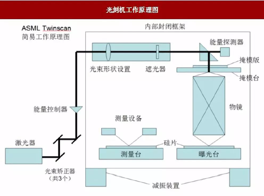
ASML's lithography machines are often referred to as TWINSCAN models, and from the operation videos, it appears that two stages are moving underneath. However, this is not two stages performing lithography simultaneously, but rather one stage performing step-and-scan lithography while the other stage is performing "pre-alignment." Pre-alignment involves scanning the areas of hundreds or thousands of dies on a wafer with a measurement tool to determine their arrangement and how many nanometers each step should be in order to align precisely. These data are recorded, and once the lithography process is finished on one stage, the pre-aligned stage is moved over and the automatic program for step-and-scan lithography is initiated according to the measured data.
To be continued...


Site Map | 萨科微 | 金航标 | Slkor | Kinghelm
RU | FR | DE | IT | ES | PT | JA | KO | AR | TR | TH | MS | VI | MG | FA | ZH-TW | HR | BG | SD| GD | SN | SM | PS | LB | KY | KU | HAW | CO | AM | UZ | TG | SU | ST | ML | KK | NY | ZU | YO | TE | TA | SO| PA| NE | MN | MI | LA | LO | KM | KN
| JW | IG | HMN | HA | EO | CEB | BS | BN | UR | HT | KA | EU | AZ | HY | YI |MK | IS | BE | CY | GA | SW | SV | AF | FA | TR | TH | MT | HU | GL | ET | NL | DA | CS | FI | EL | HI | NO | PL | RO | CA | TL | IW | LV | ID | LT | SR | SQ | SL | UK
Copyright ©2015-2025 Shenzhen Slkor Micro Semicon Co., Ltd