Service hotline
+86 0755-83044319

release time:2022-03-17Author source:SlkorBrowse:8422
Most electronic systems need some kind of conversion between the supply voltage and the circuit voltage to be supplied. When the battery loses its charge, the voltage will drop. Some DC-DC conversions can ensure that more energy stored in the battery is used to power the circuit. In addition, if we use 110 V AC lines, we can't directly supply power to semiconductors such as microcontrollers. Since almost every electronic system uses voltage converters (also known as power supplies), they have been optimized for different uses over the years. Of course, optimization goals are usually solution size, conversion efficiency, EMI and cost.
Simple power supply: LDO
One of the simple forms of power supply is low dropout (LDO) regulator. LDO is a linear regulator as opposed to switching regulator. The linear regulator places an adjustable resistor between the input voltage and the output voltage, which means that no matter how the input voltage changes, which load current is passing through the equipment, the output voltage is fixed. Figure 1 shows the basic principle of this simple voltage converter.
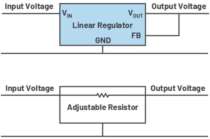
Figure 1. Linear voltage regulator converts one voltage to another.
For many years, the typical power converter is composed of a 50 Hz or 60 Hz transformer, which is connected to the power grid and generates an unstable output voltage with a certain winding ratio, which is several volts higher than the required power supply voltage in the system. Then, a linear regulator is used to convert this voltage into a stable regulated voltage required by electronic products. Figure 2 shows the block diagram of this concept.
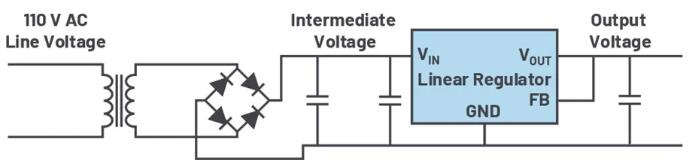
2. Line transformer followed by linear voltage regulator.
The problem with the basic setup in Figure 2 is that the 50 Hz/60 Hz transformer is relatively bulky and expensive. In addition, the linear regulator also emits a lot of heat, so the overall efficiency of the system is low, and it is difficult to eliminate the generated heat due to the high power of the system.
To avoid the disadvantages of the power supply shown in fig. 2, the switching mode power supply was invented. They do not depend on 50 Hz or 60 Hz AC voltage, but use DC voltage, sometimes rectify AC voltage, generate higher frequency AC voltage to use smaller transformer, or use LC filter to rectify voltage to generate DC output voltage in non-isolated system. The advantage is that the solution is small in size and relatively low in cost. The generated AC voltage does not need to be a sinusoidal voltage waveform. The simple PWM signal waveform of can work well, and can be easily generated by using PWM generator and switch.
Until 2000, bipolar transistors were commonly used switches. They have good performance, but the switching speed is relatively low. The efficiency is not high, and the switching frequency is limited to 50 kHz or 100 kHz. Nowadays, we use switching MOSFET instead of bipolar transistor, and the switching speed is much faster. On the other hand, the switching loss is lower, and the switching frequency is as high as 5 MHz. Such a high switching frequency enables the power stage to use very small inductance and capacitance.
Switching regulators bring many advantages. They usually provide high-efficiency voltage conversion, allow step-up and step-down, and provide a relatively compact and low-cost design. The disadvantage is that the design and optimization process is complicated, and the switching conversion and switching frequency will also produce EMI. Switching mode power supply regulator and LTpowerCAD® And LTspice® The availability of power supply design tools has greatly simplified this difficult design process. With these tools, the circuit design process of switching mode power supply can be semi-automated.
Isolation in power supply
When designing a power supply, the first question to be answered is whether electrical isolation is required. Electrical isolation is used for a number of reasons. It can improve the safety of the circuit, allow the floating system to operate, and prevent the noisy grounding current from spreading through different electronic devices in a circuit. Two common isolation topologies are flyback converter and forward converter. However, for higher power, other isolation topologies such as push-pull, half-bridge and full-bridge are used.
If electrical isolation is not required, a non-isolated topology will be used in most cases. Topology always requires a transformer, and this kind of equipment is often expensive and bulky, and off-the-shelf equipment that meets the exact requirements of customized power supply is usually hard to get.
Most common topologies when isolation is not required
The common non-isolated switching mode power supply topology is buck converter, also known as buck converter, which receives a positive input voltage and generates an output voltage lower than the input voltage. It is one of the three basic switching mode power supply topologies, and only needs two switches, one inductor and two capacitors. Figure 3 shows the basic principle of this topology. The high-end switch sends pulse current from the input terminal, and generates a switching mode voltage, which alternates between the input voltage and the ground voltage. The LC filter obtains the pulse voltage at the switch node and generates a DC output voltage. According to the duty ratio of the PWM signal of the high-end switch, different levels of DC output voltages are generated. This DC-DC buck converter has high efficiency, is relatively easy to build, and requires few components.
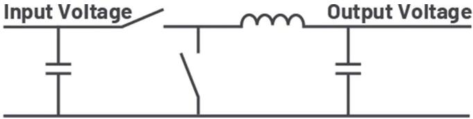
Figure 3. Concept of simple buck converter.
The buck converter emits pulse current at the input, while the output has continuous current from the inductor. This is why the noise of the buck converter is very loud at the input, but not so loud at the output. It is important to know this when designing a low noise system.
Besides the buck topology, the second basic topology is the boost topology. The boost topology uses the same five basic power elements as the buck topology, but after rearrangement, the inductor is placed at the input and the high-side switch is placed at the output. Boost topology is used to boost an input voltage to an output voltage higher than the input voltage.
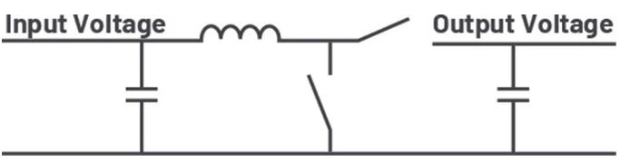
Figure 4. Concept of simple boost converter.
When choosing a boost converter, it is important to note that the maximum rated switching current is always specified in the data sheet of the boost converter, instead of the maximum output current. In the buck converter, the maximum switching current is directly related to the maximum achievable output current, and has nothing to do with the voltage ratio between the input voltage and the output voltage. In the boost regulator, the voltage ratio directly affects the possible maximum output current based on the fixed maximum switching current. When choosing the appropriate boost regulator IC, you should know not only the required output current, but also the input and output voltages designed in the development.
The noise of the boost converter at the input is very low, because the inductance consistent with the input connection can prevent the current from changing rapidly. However, at the output end, the noise of this topology is very large. We only see the pulse current flowing through the external switch, so we pay more attention to the output ripple than the buck topology.
The third basic topology is the inverting buck-boost converter, which consists of only five basic components. This converter takes a positive input voltage and converts it into a negative output voltage, hence its name. In addition, the input voltage may be higher or lower than the absolute value of the inverted output voltage. For example, the–-12 V output voltage may be generated from 5 V or 24 V at the input. This may happen without any special circuit modification. Figure 5 shows the circuit concept of the inverting buck-boost converter.
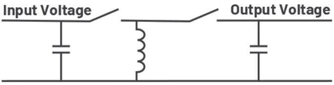
Figure 5. Concept of simple inverting buck-boost converter.
In the inverted buck-boost topology, the inductor is grounded from the switching node. There are pulse currents at the input and output of the converter, so the noise at the input and output of this topology is high. In low noise applications, this characteristic is compensated by adding additional input and output filtering.
An advantageous aspect of the inverted buck-boost topology is that any buck switching regulator IC can be used in this converter. As long as the output voltage of the buck circuit is connected to the system ground. The grounding of IC step-down circuit will become the adjusted negative voltage. This feature makes the choice of switching regulator IC in the market wide.
Special topology
Besides the three basic non-isolated switching mode power supply topologies discussed earlier, there are many topologies available. However, they all require additional power components. This usually increases the cost and reduces the power conversion efficiency. Although there are some exceptions, adding extra components in the power supply path usually increases the loss. Some common topologies include SEPIC, Zeta, UK and 4-switch buck-boost. They all have functions that the three basic topologies do not have. The following is a list of important features of each topology:
01
SEPIC:SEPIC can generate a positive output voltage from a positive input voltage higher or lower than the output voltage. Boost regulator IC can be used to design SEPIC power supply. The disadvantage of this topology is that it requires a second inductor or a coupling inductor and a SEPIC capacitor.
02
Zeta: This Zeta converter is similar to SEPIC, but can generate positive or negative output voltage. Moreover, it has no right half plane zero point (RHPZ), thus simplifying the regulation loop. The buck converter IC can be used in this topology.
03
UK: UK converter can convert positive input voltage into negative output voltage. It uses two inductors, one at the input and one at the output, so the noise at the input and output is very low. The disadvantage is that there are not many switching mode power conversion IC's that support this topology, because the regulation loop needs negative voltage feedback pins.
04
4Switching buck-boost: This type of converter has become very popular in recent years. It provides a positive output voltage from a positive input voltage. The input voltage may be higher or lower than the regulated output voltage. This converter has higher power conversion efficiency and only needs one inductor, so it replaces many SEPIC designs.Common isolation topology
Flyback converters are usually used for power levels up to 60 W. The working mode of the circuit is that the electric energy is stored in the transformer during the conduction time. When disconnected, the electric energy is released to the secondary side of the converter to supply power for the output. This converter is easy to build, but requires a relatively large transformer to store all the electric energy required for normal operation. On the one hand, this topology is limited to a lower power level. Figure 6 shows the flyback converter at the top and the forward converter at the bottom.
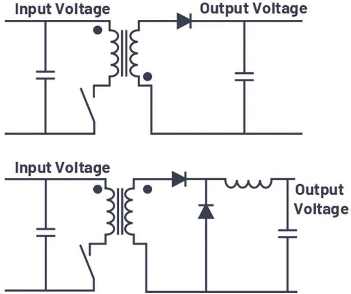
6. Flyback converter (top) and forward converter (bottom).
Besides flyback converter, forward converter is also very popular. It uses a transformer in a different way than a flyback converter. During the conduction time, although the current flows through the primary winding, the current also flows through the secondary winding. Electric energy should not be stored in the transformer coil. After each switching cycle, we must ensure that all magnetization of the coil is released to zero, so that the transformer will not be saturated after several switching cycles. Several different technologies can be used to release electric energy from the coil. A common way is to use an active clamp with small extra switches and capacitors.
Fig. 7 shows the schematic diagram of LTspice simulation environment with active clamp forward design using ADP1074. In the forward converter, there is an extra inductance in the output path that is not found in the flyback converter, as shown in Figure 6. Although this additional component has the related space and cost impact, it helps to produce a lower noise output voltage compared with the flyback converter. In addition, at the same power level as the flyback converter, the transformer size required by the forward converter may be much smaller.
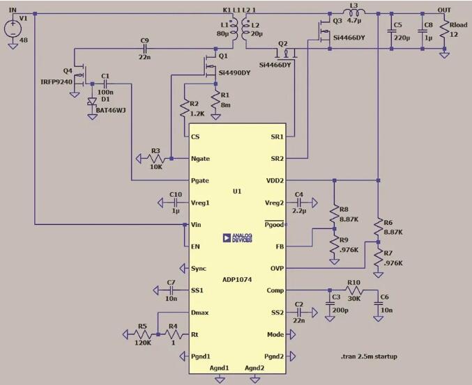
Figure 7. Active clamp forward circuit using ADP1074 to generate isolated output voltage, as shown in the simulation in LTspice.
Advanced isolation topology
Besides flyback and forward topology, there are many concepts of electrical isolation converters based on different transformers. The following list gives some basic explanations of common converters:
Half-bridge/full-bridge: These two topologies are usually used for higher power designs, starting from several hundred watts and going all the way to several kilowatts. Besides low-side switches, they also need high-side switches, but they can achieve high power transmission through relatively small transformers.
ZVS: This term is usually mentioned when discussing high-power isolated converters. It stands for Zero Voltage Switching. Another term for this type of converter is LLC (Inductance-Inductance-Capacitance) converter. The purpose of these architectures is to achieve efficient conversion. They will produce resonant circuits and switch the power switch when the voltage or current on the switch approaches zero. In this way, the switching loss is minimized. However, this kind of design is difficult to realize, and the switching frequency is not fixed, sometimes causing EMI problems.
Switched capacitor converter
Besides linear regulators and switched mode power supplies, there is a third group of power converters: switched capacitor converters. Also known as charge pump. They use switches and capacitors to multiply or invert voltages. A big advantage is that it doesn't need any inductance. This type of converter is usually used for low power levels below 5 W. However, the recent significant progress allows for more powerful switched capacitor converters. Fig. 8 shows LTC7820 with 98.5% efficiency and 120 W design, which converts 48 V to 24 V.
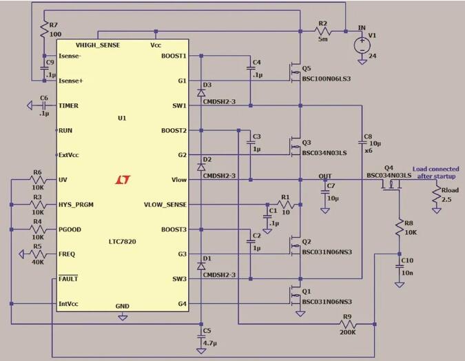
Figure 8. LTC7820 Fixed Ratio High Power Charge Pump DC-DC Controller.
Digital power supply
The first is the digital interface, through which the electronic system can communicate with the power supply. Different parameters can be set instantly to optimize the power supply for different working conditions. In addition, the power supply can also communicate with the main processor and cause a warning or fault sign. For example, the system can easily monitor the load current, exceed the preset threshold or the battery temperature is too high.
The second digital building module uses digital loop instead of analog regulating loop. This works well, but for most applications, it's best to adopt a standard analog feedback loop that has a certain digital influence on some parameters, such as adjusting the gain of error amplifier immediately or dynamically setting the loop compensation parameters to realize a stable but fast feedback loop.
An example of a device with a purely digital control loop is ADI's ADP1046A. An example of digital interface buck regulator optimized by digital influence and with analog control loop is LTC3883.
EMI considerations
Electromagnetic interference (EMI) has always been a problem that should be paid attention to when designing switching mode power supply. The reason is that the switching mode power supply will switch high current in a short time. The faster the switching speed, the better the overall efficiency of the system. Faster switching speed can reduce the time of partially turning on the switch. During this part of the on time, most of the switching losses will occur. Figure 9 shows the waveform of the switching mode power supply at the switching node. Take the buck regulator as an example. High voltage is defined by the current through the high-side switch, while low voltage is defined by no current flowing through the high-side switch.
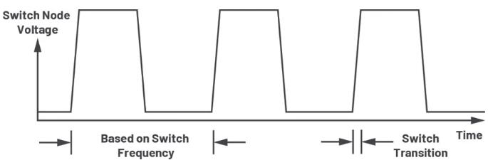
Figure 9. Switching speed and switching frequency of switching mode power supply.
As can be seen in fig. 9, the noise generated by the switching mode power supply comes not only from the adjusted switching frequency, but also from the switching speed which is much higher than the frequency. Although the switching frequency usually runs between 500 kHz and 3 MHz, the switching time may be several nanoseconds long. In 1 ns switching time, the corresponding frequency in the spectrum will be 1 GHz. At least these two frequencies will be regarded as electromagnetic radiation disturbance and conducted radiation. The oscillation of the regulating loop or the interaction between the power supply and the filter may also bring other frequencies.
There are two reasons to reduce EMI. The first reason is to protect the function of an electronic system powered by a specific power supply. For example, the 16-bit ADC used in the system signal path should not pick up the switching noise from the power supply; The second reason is to meet some EMI regulations formulated by governments all over the world to protect the reliable functions of different electronic systems at the same time.
There are two forms of EMI, radiated EMI and conducted EMI. The effective way to reduce radiated EMI is to optimize the layout of PCB, and to adopt such technologies as Silent Switcher® of ADI. Such technology. Of course, it is also effective to put the circuit in a shielded metal box. However, this may not be practical, and in most cases it is costly.
Conducted EMI is usually attenuated by additional filtering. Next, additional filtering to reduce conducted radiation will be discussed.
filter waves
The RC filter is a basic low-pass filter. However, in the power supply design, each filter is an LC filter. Generally, it is enough to add some inductors in series, because it will form an LC or CLC filter together with the input or output capacitance of the switching mode power supply. Sometimes only capacitors are used as filters, but considering the parasitic inductance of power lines or traces, we combine capacitors to form an LC filter. The inductor l may be an inductor with a coil or a ferrite bead. The purpose of LC filter is actually a low-pass effect, which allows DC power to pass through and attenuates high frequency interference to a great extent. The LC filter has a double pole, so it can achieve a high frequency attenuation of 40 dB/ octave. The filter can achieve a relatively sharp frequency drop. Designing filters is not easy; However, because parasitic components of the circuit (such as trace inductance) will produce effects, modeling the filter also needs to model the main parasitic effects. This makes the analog filter quite time-consuming. Many designers with experience in filter design know which filters work well, and may iteratively optimize a filter to obtain a new design.
When designing all filters, it is necessary to consider not only the small signal behavior, such as the transfer function of the filter in Porter diagram, but also the large signal effect. In any LC filter, the power supply will pass through the inductor. If the power supply is no longer needed at the output, the electric energy stored in the inductor needs to be released somewhere due to sudden load transient. It will charge the capacitor of the filter. If the filter is not designed for this worst case, the stored electric energy may cause voltage overshoot, which may damage the circuit.
Finally, the filter has a certain impedance. This impedance interacts with the impedance of the power converter attached to the filter. This interaction may lead to instability and oscillation. Analog devices' simulation tools such as LTspice and LTpowerCAD are helpful to answer all these questions and design excellent filters. Figure 10 shows the graphical user interface of filter designers in LTpowerCAD design environment. Using this tool to design filters is very simple.
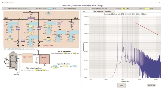
Figure 10. Design of input filter of buck regulator using LTpowerCAD.
Silent Switchers
Electromagnetic interference is hard to stop. A special shield made of a certain metal material is required. The cost of doing so is very high. For a long time, engineers have been looking for ways to reduce electromagnetic radiation disturbance caused by switching mode power supply. A few years ago, Silent Switcher technology made a major breakthrough. By reducing the parasitic inductance in the thermal circuit of the switching mode power supply, and dividing the thermal circuit into two circuits, which are arranged in a highly symmetrical way, the electromagnetic radiation disturbances mostly cancel each other out. Today, many Silent Switcher devices provide much lower electromagnetic radiation disturbance than traditional products. Reducing electromagnetic radiation disturbance can improve switching speed without serious EMI. Increasing the switching speed can reduce the switching loss, thus increasing the switching frequency. An example of this innovation is LTC3310S, which has a switching frequency of 5 MHz and uses low-cost external components to achieve a very compact design.
Power management is necessary, but it can also be fun.
In this paper, we discuss many aspects of power supply design, including different power supply topologies and their advantages and disadvantages. This information is very basic for power engineers, but for experts and non-professionals, it is helpful to use software tools such as LTpowerCAD and LTspice in the design process. With these tools, the power converter can be designed and optimized in a short time.
Disclaimer: This article is reproduced from the "Power R&D Alliance". This article only represents the author's personal views, and does not represent the views of Sacco Micro and the industry. It is only for reprinting and sharing to support the protection of intellectual property rights. Please indicate the original source and author when reprinting. If there is any infringement, please contact us to delete it.
Company Tel: +86-0755-83044319
Fax/fax:+86-0755-83975897
Email: 1615456225@qq.com
QQ: 3518641314 Manager Li
QQ: 332496225 Manager Qiu
Address: Room 809, Block C, Zhantao Technology Building, No.1079 Minzhi Avenue, Longhua New District, Shenzhen


Site Map | 萨科微 | 金航标 | Slkor | Kinghelm
RU | FR | DE | IT | ES | PT | JA | KO | AR | TR | TH | MS | VI | MG | FA | ZH-TW | HR | BG | SD| GD | SN | SM | PS | LB | KY | KU | HAW | CO | AM | UZ | TG | SU | ST | ML | KK | NY | ZU | YO | TE | TA | SO| PA| NE | MN | MI | LA | LO | KM | KN
| JW | IG | HMN | HA | EO | CEB | BS | BN | UR | HT | KA | EU | AZ | HY | YI |MK | IS | BE | CY | GA | SW | SV | AF | FA | TR | TH | MT | HU | GL | ET | NL | DA | CS | FI | EL | HI | NO | PL | RO | CA | TL | IW | LV | ID | LT | SR | SQ | SL | UK
Copyright ©2015-2025 Shenzhen Slkor Micro Semicon Co., Ltd
