Including system design and verification, integrated circuits, PCB and other fields, the performance of Electronic Design Automation, EDA) tools and the development of the market itself play a vital role. By the end of 2021, there will be a total of 35 billion IoT devices in the world. From the downstream application side, the demand for EDA software will continue to grow.
 注:全球 EDA 工具市场增长趋势图 "Electronic Design Automation (EDA) industry will exceed $20 billion in 2027."
 ——Global Market Insights Inc.
With the vigorous development of the Internet of Things market, there are some new changes in EDA industry that deserve our attention. #1
The demand for EDA in the medical device industry has increased significantly. The introduction of new technologies in the medical industry continues, and the use of new equipment, new instruments and new tools makes it possible to treat and operate seemingly impossible in the past. It is precisely because of the introduction of EDA that the most well-known endoscopic and laparoscopic surgery can benefit countless patients. GE, ABB, Siemens and many other big manufacturers are also able to produce high-performance artificial intelligence devices for disease diagnosis and treatment just because of EDA software.
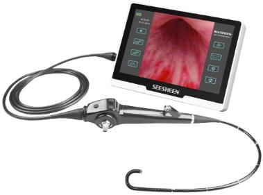
Note: EDA tools are widely used in endoscopic equipment and surgical procedures. EDA software company also continuously iterates machine learning algorithms to improve the performance of chip design tools. Ibex Medical Diagnostics and KSM recently announced that they started to use Galen Gastronomy, a diagnostic and quality control tool with AI capabilities, to detect possible cancer risks in gastrointestinal tract. #2
Miniaturization is becoming more and more popular. As the values held by everyone in the electronic industry say, "Smaller means stronger." Miniaturization, light weight, traditional large-scale equipment through the way of continuous miniaturization, so that electronic products can continue to penetrate into more and more rich scenes. In the fields of automotive electronics, medical automation and consumer electronics, it is still the trend of product iteration and cost-down to use smaller and more beautiful devices with higher integration and more powerful functions.

Note: The pursuit of size of wearable devices is forcing the progress of EDA tools. Because of the continuous influence of this "small is beautiful" wave, mobile phones are becoming thinner and lighter, and tablets, PCs, nano-scale products of wearable devices and medical devices are becoming more and more popular in the homes of ordinary people. If this trend continues, the market demand for EDA will undoubtedly continue to increase. #3
High-end manufacturing puts forward new requirements for EDA. For most people, high-end manufacturing is directly equal to the use of robots and automated assembly line. However, at present, the robots in the workshop are more responsible for "manual work" such as picking and placing, testing and packaging, and material ordering. As all kinds of equipment become more and more streamlined, the production links of electronic products will become more and more sophisticated, which puts forward new requirements for the accuracy of the traditional "five big and three thick" robotic arm.

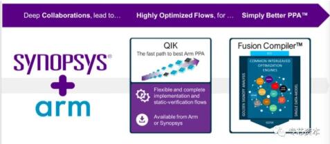
Note: Synopsys is located at the headquarters of Mountain View, California. Synopsys, the world's leading EDA software and semiconductor IP company, recently joined forces with TSMC. TSMC will use Sysopsys' EDA software in its latest version of 3 nm process DRM and SPICE production line. The chips produced by this production line will be used in mobile devices, 5G and other artificial intelligence scenarios. #4
The online scene continues to accelerate. With the continuous discussion of the topic of digital transformation, EDA software companies also pay more attention to the optimization of online platforms, thus empowering business processes. Compared with previous semiconductor companies that used preset data parameters to verify chip design, the current EDA enabling workflow is more flexible, which can realize design, simulation and verification, and can also play a greater role in chip trial production and mass production. If EDA software is connected to the cloud, the cost will be more friendly and the existing data center resources will be less occupied.
Note: ARM and Synopsys have reached a strategic cooperation. A few months ago, ARM announced that it would upgrade its EDA software, so as to better plan storage resources and computing power, and at the same time achieve the purpose of reducing costs. Compared with buying more servers and other software equipment, ARM's recognition of EDA, especially the practice of connecting EDA with the cloud, has caused a whirlwind in the semiconductor industry. Soul asks: Why is China's EDA software lagging behind? The backwardness of EDA industry can be described as "Achilles heel" for the development of China's IC industry. Looking around the world, the EDA alliance formed by the American Big Three and American-funded related enterprises has become a constraint to all chip markets including China. It is no exaggeration to say that the EDA tools used in the design and verification of all Chinese "self-developed" chips are basically from the United States.
If Chinese chip companies want to participate in global competition, they have to solve the current problems of EDA software. Although many companies including Xiaomi have participated in the research and development of EDA tools, we haven't seen much progress in the open market.
In fact, as early as the mid-1980s, the Panda chip design system appeared in China. However, there are few companies using this system in the market, so its performance is questionable. At present, there are more EDA manufacturers in the Chinese market, including Huada Jiutian, Chips and Semiconductors.
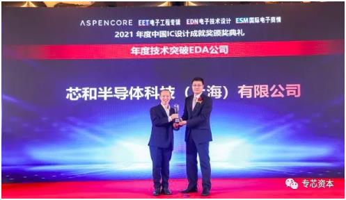
Note: Core and Semiconductor won the annual technical breakthrough EDA company award.
Unfortunately, none of these vendors can realize the software delivery of the whole design process. So why does China's EDA software lag behind the United States? There are four reasons for this:First, the lack of a complete set of programs makes it impossible to participate in the whole process competition. At present, most EDA software in China is still in the stage of specializing in one or several links, and it has failed to form a complete set of alternative product matrix. However, digital design processes are mostly monopolized by Synopsys and Cadence. Even if Chinese manufacturers can cut into some links, it is difficult to shake the control of the American Big Three in all links. Therefore, Chinese manufacturers need to launch a complete set of solutions in order to compete with international manufacturers in the same dimension. However, there are other difficulties and challenges in this process.

Note: Three American EDA giants 二、Shortage of talents, the industry failed to attract EDA talents. Most of China's EDA tool development engineers work for the Big Three in the United States. It is reported that among more than 1,500 EDA engineers in China, less than 300 work for domestic EDA companies. Synopsys, a company in the United States, has more than 5,000 employees worldwide. Under the background of the booming domestic mobile Internet market, these engineers prefer to go to companies such as Alibaba Tencent, rather than struggling in the domestic EDA companies. 三、The market entry threshold is high, it is difficult to enter the market, and it is even more difficult to break the market. 95% of China's EDA market belongs to America's three giants, which is a cruel market for any domestic and foreign EDA suppliers. Even if Chinese manufacturers can develop a complete set of solutions, it is difficult to pose a threat to the Big Three in a short time. At present, many engineers in chip companies use the solutions of the Big Three in universities. After entering the new company, their choice preference makes small domestic factories unattractive. 四、Lack of integration of advanced process nodes, losing step by step.
The connection between the design process and the production process is very important for EDA process. The close connection between the three giants, the head wafer and the foundry enables them to deeply understand each link. This kind of stickiness is what domestic manufacturers need to continuously track and follow up while launching solutions.
Disclaimer: This article is reproduced from "Special Core Capital". This article only represents the author's personal views, not those of Sacco Micro and the industry. It is only for reprinting and sharing to support the protection of intellectual property rights. Please indicate the original source and author when reprinting. If there is any infringement, please contact us to delete it.
Company Tel: +86-0755-83044319
Fax/fax:+86-0755-83975897
Email: 1615456225@qq.com
QQ: 3518641314 Manager Li
QQ: 332496225 Manager Qiu
Address: Room 809, Block C, Zhantao Technology Building, No.1079 Minzhi Avenue, Longhua New District, Shenzhen