Service hotline
+86 0755-83044319

release time:2025-05-09Author source:SlkorBrowse:1479
As electronic devices become increasingly smaller and operate at higher frequencies, electrostatic discharge (ESD) protection has become a core challenge in circuit design. Although ESD events are brief (on the nanosecond scale), they can release thousands of volts, causing irreversible damage to delicate chips. As the "invisible guardian" in protective components, the ESD diode must strike a precise balance between low capacitance, fast response, and high reliability. This article will take the GBLC12CI as an example, analyzing how it meets the demanding requirements of modern electronic devices through parameter optimization.
1. VRWM=12V: Precise Setting of Reverse Working Voltage
VRWM (Reverse Working Voltage) defines the maximum reverse voltage the device can handle in normal operation. The 12V parameter of the GBLC12CI indicates that when the circuit’s operating voltage is below this value, the diode remains in a high-impedance state with a leakage current (IR) of only 1μA, making it negligible in terms of signal integrity. This design is particularly suitable for interfaces with supply voltages below 12V, such as USB 3.0 and HDMI 2.1, preventing false activation of the protection mechanism due to voltage fluctuations.
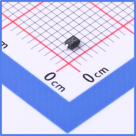
Slkor Electrostatic Discharge Diode GBLC12CI product photo
2. VBR min=13.3V: Tolerance Control of Breakdown Voltage
VBR (Breakdown Voltage) is the critical voltage at which the device switches from high-impedance to conduction state. The minimum breakdown voltage of 13.3V (with typical values often higher) means that when the ESD pulse voltage exceeds this threshold, the diode quickly enters avalanche breakdown mode, providing a low-impedance path for transient currents. Compared to fixed breakdown voltage designs, this 13.3V minimum ensures consistency across different product batches, reducing the risk of protection failure due to parameter variations.
Slkor Electrostatic Discharge Diode GBLC12CI specification
3. VC=24V: Dynamic Clamping Voltage Suppression
Clamping Voltage defines the device's ability to limit voltage to a safe threshold during an ESD event. Under IEC 61000-4-2 standard testing (±8kV contact discharge), the GBLC12CI can clamp transient voltages to below 24V. This parameter directly determines the protection margin for the protected chip: for example, in a digital circuit powered by 5V, a 24V clamping voltage provides a 19V protection window, significantly higher than typical ESD event strengths.
Parameters of Slkor Electrostatic Discharge Diode GBLC12CI
4. CJ=0.8pF: Ultra-Low Junction Capacitance
Junction capacitance is a critical parameter for high-speed signal interfaces. The ultra-low 0.8pF capacitance design of the GBLC12CI allows seamless integration into high-frequency lines like USB 3.2 Gen 2 (10Gbps) and MIPI D-PHY (1.5Gbps/lane). By optimizing doping concentration and the PN junction structure, its capacitance is reduced by more than 50% compared to traditional ESD devices, effectively reducing signal attenuation and reflection, ensuring compliance with eye diagram quality standards.
5. SOD-323 Package: A Revolution in Space Efficiency
The SOD-323 package (2.5mm × 1.25mm) is one-third the size of the SOT-23 package but can handle pulse power up to 1.5kW (8/20μs). This feature makes it an ideal choice for space-constrained applications such as wearable devices and TWS earbuds, while also being compatible with automatic surface-mount assembly processes to improve production efficiency.
1. Dynamic Response Mechanism
The GBLC12CI uses an improved TVS (Transient Voltage Suppression) structure, combining a low-doping drift region and multi-zone doping technology to achieve a nanosecond-level response time (<1ns). When an ESD pulse occurs, the device switches from high to low impedance within 1ns, much faster than the internal protection circuits of ICs, ensuring the reliability of the first line of [敏感词].
2. Balancing Leakage Current and Reliability
The extremely low reverse leakage current (IR) of 1μA is achieved by optimizing the surface passivation layer and field-limiting ring structure. Even in harsh environments with 85°C/85%RH, IR remains below 5μA, preventing long-term operation-induced DC offset or battery life degradation.
3. Thermal Management and Power Dissipation
Despite the small size of the SOD-323 package, its thermal resistance (θJA) is kept below 250°C/W through a three-dimensional stacked structure and high-conductivity silver paste. Under a single 8kV ESD pulse, the junction temperature rise is only about 15°C, meeting AEC-Q101 automotive-grade reliability standards.
1. Portable Device Interfaces
In the USB-C/Lightning interfaces of smartphones and tablets, the GBLC12CI protects both data lines (D+/D-) and power lines (VBUS), with its 0.8pF capacitance ensuring 480Mbps high-speed transmission without loss.
2. Wearable Device Antenna Ports
Bluetooth 5.3, Wi-Fi 6E, and other 2.4GHz/5GHz RF lines are sensitive to parasitic capacitance. The 0.8pF junction capacitance ensures insertion loss (S21) is below 0.5dB at frequencies below 6GHz, safeguarding wireless performance.
3. Automotive Electronics High-Speed Buses
For in-vehicle Ethernet (100BASE-T1/1000BASE-T1), the GBLC12CI’s operating temperature range of -55°C to 150°C and sulfur resistance make it capable of handling the extreme conditions found in engine compartments.
Through precise parameter tuning, the GBLC12CI sets a new benchmark in ESD protection: its 12V working voltage suits mainstream consumer electronics, 24V clamping voltage offers ample safety margin, 0.8pF capacitance breaks through the bottleneck of high-speed interfaces, and the SOD-323 package defines a new standard for space efficiency. Its design philosophy reveals the evolutionary direction of modern electronic protection devices—achieving collaborative optimization of electrical, thermal, and mechanical properties at the microscopic scale. As 5G, IoT, and automotive electronics continue to advance, such "small but exquisite" components will become key pillars in ensuring system robustness.
Slkor has research and development offices in Busan, South Korea, Beijing, China, and Suzhou, China. Most of the wafer manufacturing and packaging and testing are carried out within China. The company employs and collaborates with individuals and organizations worldwide, with a laboratory for product performance and reliability testing and a central warehouse located at its headquarters in Shenzhen. Slkor has filed for over a hundred invention patents, offers more than 2,000 product models, and serves over ten thousand customers globally. Its products are exported to countries and regions including Europe, the Americas, Southeast Asia, and the Middle East, making it one of the rapidly growing semiconductor companies in recent years. With well-established management systems and streamlined workflows, Slkor has rapidly enhanced the brand awareness and reputation of its "SLKOR" brand through its outstanding quality and standardized services. Its product range includes three major series: diodes, transistors, and power devices, with recent introductions of new products such as Hall elements and analog devices, expanding its presence in sensors, Risc-v microcontrollers, and other product categories.


Site Map | 萨科微 | 金航标 | Slkor | Kinghelm
RU | FR | DE | IT | ES | PT | JA | KO | AR | TR | TH | MS | VI | MG | FA | ZH-TW | HR | BG | SD| GD | SN | SM | PS | LB | KY | KU | HAW | CO | AM | UZ | TG | SU | ST | ML | KK | NY | ZU | YO | TE | TA | SO| PA| NE | MN | MI | LA | LO | KM | KN
| JW | IG | HMN | HA | EO | CEB | BS | BN | UR | HT | KA | EU | AZ | HY | YI |MK | IS | BE | CY | GA | SW | SV | AF | FA | TR | TH | MT | HU | GL | ET | NL | DA | CS | FI | EL | HI | NO | PL | RO | CA | TL | IW | LV | ID | LT | SR | SQ | SL | UK
Copyright ©2015-2025 Shenzhen Slkor Micro Semicon Co., Ltd
