

Service Hotline
Blogs

Blogs

1SS357 Schottky Diode: Ultra-Low Conduction Loss, Specialized Device for Micro Small-Signal Switching
2026-07-28
51
As smart wearable devices, micro sensors, wireless Bluetooth modules and portable testing equipment continuously evolve toward ultra-miniaturization, ultra-low power consumption and high-frequency signal switching, small-signal Schottky diodes have become essential core components for weak-signal rectification, voltage clamping, anti-reverse connection and high-frequency freewheeling circuits. Developed by Slkor, the 1SS357 surface-mount Schottky diode adopts an ultra-small SOD-323 surface-mount package built with optimized metal-semiconductor barrier technology. Featuring three core strengths — ultra-low forward voltage drop, tiny leakage current and ultra-fast switching, it provides a lightweight, low-power and highly reliable standard solution for 40V, 100mA-class micro signal circuits.
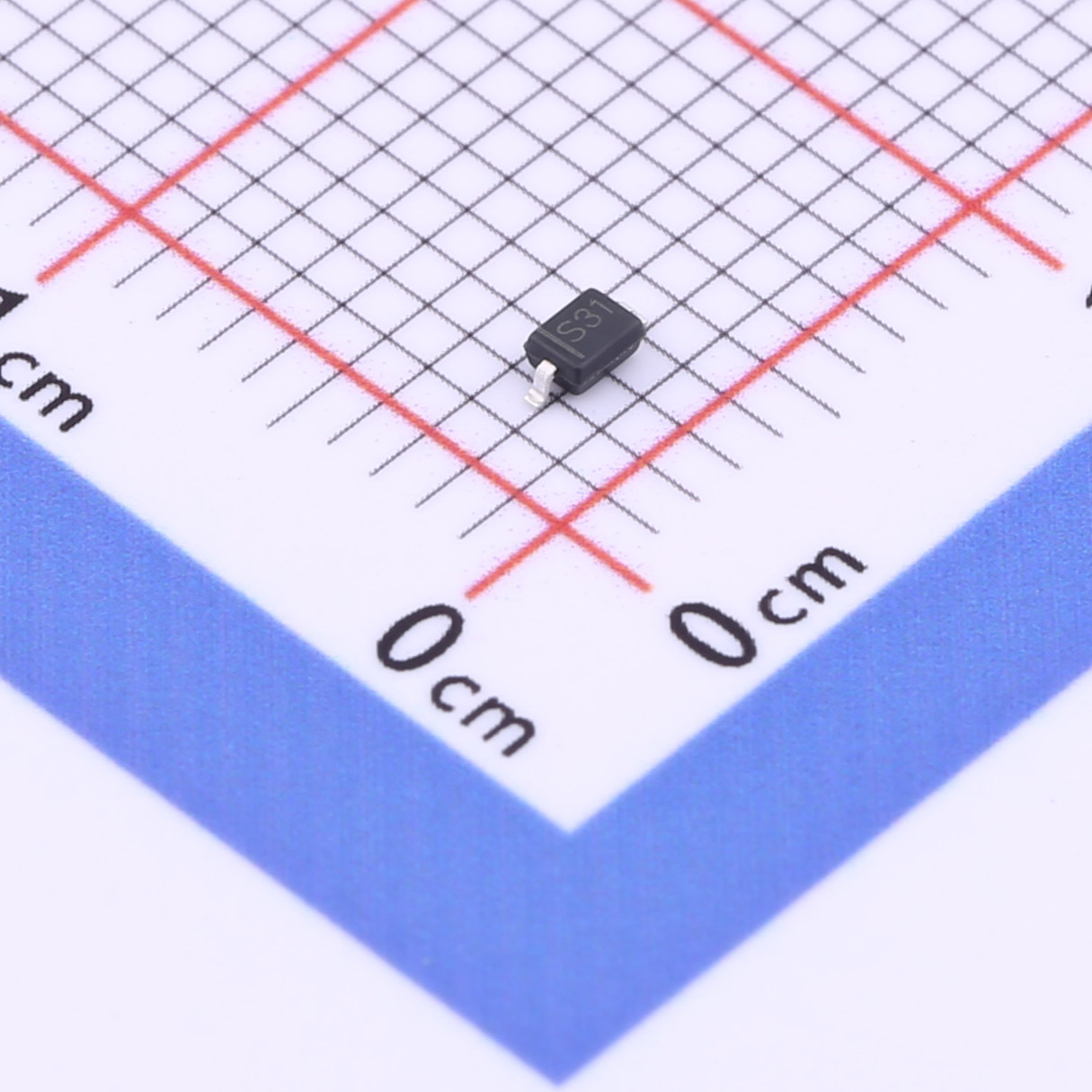
Physical photo of 1SS357 tiny package
Ultra-Low Forward Voltage Drop Enables Ultra-Low Power Energy-Saving Design
For battery-powered micro devices, conduction loss under weak current directly determines the static power consumption and service life of the whole equipment. The key electrical parameters of 1SS357 are as follows:
DC Reverse Voltage (Vr): 40V
Average Rectified Current (Io): 100mA
Forward Voltage Drop (Vf): 0.35V @ 1mA
Reverse Current (Ir): 5μA @ 40V
Package: SOD-323
Conventional small-signal diodes generally have a forward voltage drop exceeding 0.5V at a weak operating current of 1mA, leading to high conduction loss and continuous battery power consumption. In contrast, the 1SS357 achieves an ultra-low forward voltage drop of 0.35V under a tiny current of only 1mA, with negligible heat generation during conduction. Applied in indicator circuits of smart bands, wireless sensor signal rectification and anti-reverse circuits for Bluetooth module power supplies, this device requires no additional heat dissipation structures. It greatly saves PCB routing space, reduces overall static power consumption, and effectively extends the single-cycle service life of button cells and small-capacity lithium batteries, perfectly meeting the design requirements of low-power miniature electronic products.
Ultra-Fast Switching Characteristics Adapt to High-Frequency Weak Signal Processing
As a Schottky device conducting via majority carriers, the 1SS357 barely has charge storage effect with near-zero reverse recovery time and zero delay during high-frequency switching. When traditional PN-junction diodes process high-frequency weak signals, they tend to generate voltage spikes and signal distortion, interfering with sensor acquisition accuracy. Benefiting from fast switching performance, the 1SS357 can complete signal rectification, voltage level clamping and high-frequency freewheeling actions cleanly. It is widely used in high-frequency small-signal scenarios such as infrared sensing probes, wireless transceiver modules and miniature PWM dimming control, ensuring complete and distortion-free transmission of weak sensing signals and avoiding electromagnetic clutter interfering with detection data.
Low Leakage Current & Wide-Temperature Stability for Long-Term Reliable Operation
Long-term device stability is a core guarantee for wearable and outdoor micro sensors. The 1SS357 undergoes rigorous tests including wafer screening, package aging, high-low temperature cycling, voltage withstand and leakage testing to deliver stable and controllable performance under all working conditions:
- Sufficient 40V reverse voltage rating: Compatible with a full range of micro low-voltage circuits at 3.3V, 5V and 12V. Ample voltage margin resists instantaneous circuit surges and prevents damage caused by reverse breakdown.
- Minimal reverse leakage current: Only 5μA at rated reverse voltage of 40V, resulting in ultra-low leakage loss during device standby and substantially reducing static battery drain.
- Suitable for low-current loads: Rated average rectified current of 100mA with peak surge current up to 1A, easily coping with inrush current during LED power-on and instantaneous sensor startup.
- Ultra-wide operating temperature range: Stable operation from -55℃ to +125℃ with minimal parameter drift of forward voltage drop and leakage current under high and low temperatures.
- SOD-323 micro surface-mount package: Compact and thin, moisture & heat resistant, fully RoHS lead-free compliant, compatible with automatic high-speed SMT assembly and satisfying high-density miniaturized PCB routing requirements.
When deployed in smart watches, wireless temperature and humidity sensors, miniature automotive indicator lights and handheld portable testing instruments, the device maintains stable performance without degradation or abnormal rise of leakage current even under long-term frequent start-stop and ambient temperature fluctuations, continuously safeguarding the safe operation of micro precision circuits.
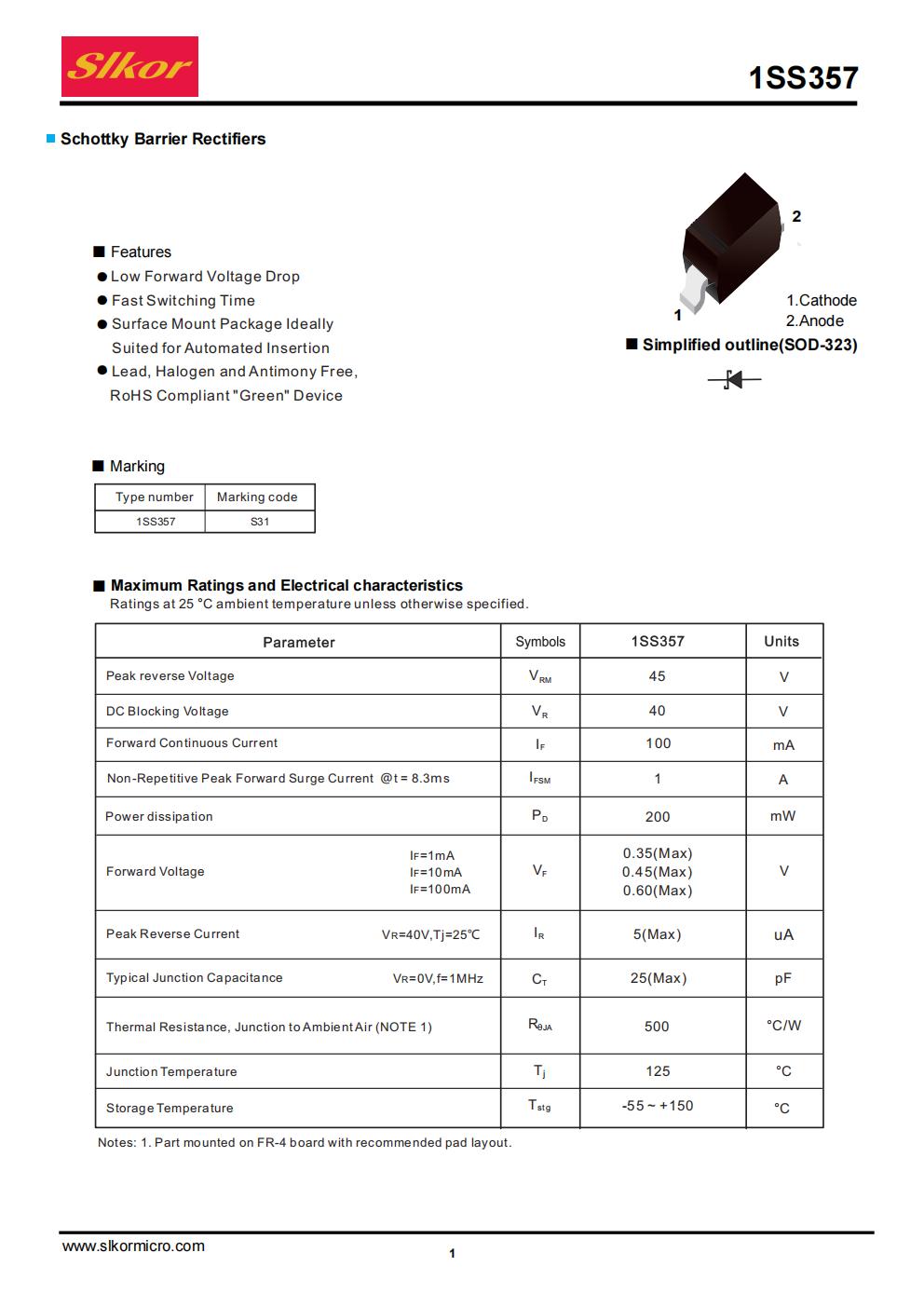
Official Datasheet Diagram of 1SS357
Official Datasheet Diagram of 1SS357
Diverse Application Scenarios Covering All Types of Micro Small-Signal Circuits
Equipped with an ultra-small package and well-balanced low-power parameters, the 1SS357 is tailor-made for low-voltage small-signal circuits, covering four mainstream application fields:
- Wearable consumer electronics: Power anti-reverse protection and weak rectification for LED backlights in smart bands, Bluetooth earphones and smart watches;
- Micro sensor equipment: Signal rectification and clamping for infrared human body sensors, wireless temperature & humidity sensors and Bluetooth BLE modules;
- Small signal control: MCU GPIO voltage level protection, low-speed digital logic and freewheeling drive for miniature indicator lights;
- Automotive & portable instruments: Miniature automotive ambient lights, handheld detection probes and small lithium battery protection circuits.
Practical Engineering Design Tips to Maximize Device Performance
- Reserve sufficient parameter safety margin: Control the peak voltage of circuits within 32V under normal operation, and limit long-term continuous operating current to no more than 70mA to reduce long-term load and extend service life.
- PCB heat dissipation optimization: When operating close to the 100mA full load for a long time, widen the pads at both ends of the diode and add local copper pour to suppress the rise of forward voltage drop caused by temperature increase.
- High-frequency routing optimization: Keep the traces of the diode anode and cathode as short and concise as possible to reduce parasitic inductance and lower voltage spikes generated during high-frequency switching.
- Reference official datasheets: Consult the official Slkor datasheet of 1SS357 before formal circuit design, and match circuit parameters against characteristic curves according to actual operating voltage and current.
Related Recommendations





 粤公网安备44030002007346号