
























Service Hotline
Blogs

Blogs

SL3139K P-Channel Low-Voltage MOSFET :Ultra-Miniature Ultra-Low Threshold Precision Switching Device
2026-08-25
73
With the continuous upgrading of consumer electronics, wearable devices and micro smart sensors toward thinner, lighter and more miniaturized designs, circuit design imposes higher requirements on the size, driving sensitivity and power consumption control of switching components. The SL3139K is a P-channel enhancement-mode low-voltage MOSFET developed by Slkor Semiconductor with advanced trench technology. Adopting an ultra-compact SOT-723 package, it features 20V withstand voltage, 0.66A rated current, ultra-low on-resistance and extremely low gate threshold voltage. Benefiting from ultra-small size, sensitive driving, ultra-low power consumption and wide compatibility, it perfectly fits high-density miniature PCB designs and serves as a cost-effective domestic alternative for small-signal switching, low-voltage power control and battery management applications.
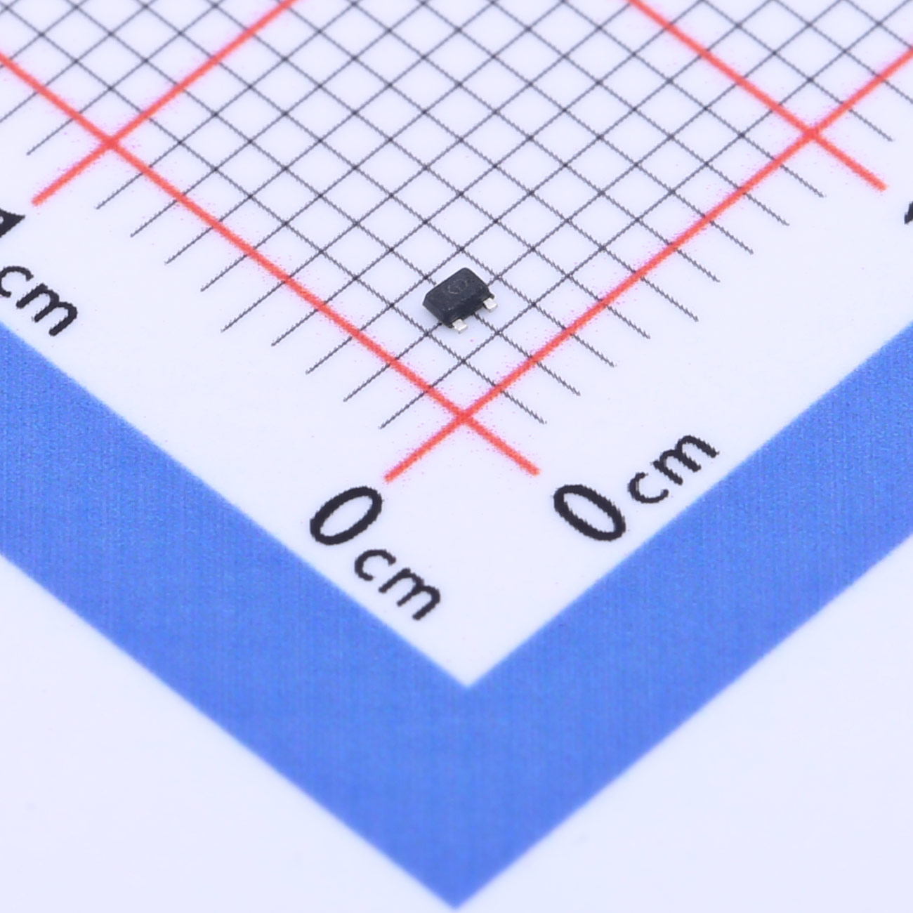
1. Core Electrical Parameters
Device Type: P-Channel Enhancement Mode MOSFET Package: SOT-723 Drain-Source Breakdown Voltage (VDSS): 20V Continuous Drain Current (Id): 0.66A On-Resistance (RDSON): 520mΩ @ VGS=4.5V, ID=1A Gate Threshold Voltage (VTH): 0.45V @ 250μA
2. Core Product Advantages
2.1 Ultra-Miniature Package for Ultra-Thin and Lightweight Devices
Packaged in industry-standard ultra-small SOT-723 form factor, the SL3139K occupies minimal PCB area and greatly saves layout space. Compared with traditional MOSFET packages, it is more suitable for space-constrained products such as earphones, smart bracelets, micro sensors and ultra-thin small home appliances, supporting the miniaturization and lightweight iteration of terminal equipment.
2.2 Ultra-Low Threshold Voltage for Sensitive Low-Voltage Driving
Featuring an ultra-low gate threshold voltage of 0.45V, the SL3139K can be directly driven by low-voltage MCUs, logic circuits and single-chip microcomputers without additional drive amplifier circuits, greatly simplifying peripheral circuit design. It delivers fast start-stop response and precise control, perfectly matching low-voltage and low-power intelligent control scenarios.
2.3 Stable Conduction Performance with Low Loss and Low Heat Generation
At a standard driving voltage of 4.5V, the ultra-low on-resistance of 520mΩ ensures low conduction loss and minimal heat generation during operation. It maintains stable performance under long-term continuous switching conditions, effectively reducing static and dynamic power consumption of terminal devices, improving battery life and operational stability, and adapting to long-term low-load and frequent switching working conditions.
2.4 P-Channel Architecture for High-End Power Reverse Control
Adopting classic P-channel design, the device is ideal for positive power switch control, power anti-reverse connection and battery charge and discharge management. It compensates for the application limitations of N-channel MOSFETs in high-end power control, providing stronger circuit compatibility and more flexible design solutions.
2.5 Mature Domestic Process with Stable Mass Production Quality
Based on Slkor’s mature trench semiconductor manufacturing process, the SL3139K features minor parameter deviation, low leakage current, strong anti-interference capability, excellent high-temperature resistance and aging resistance for long-term stable operation. Fully verified in mass production, it matches the quality level of imported mainstream devices and can directly replace overseas products in 99% of application scenarios without additional testing, fully supporting industrial mass production.
3. Main Application Fields
Leveraging its ultra-small size, ultra-low threshold, low power consumption and high-sensitivity switching performance, the SL3139K is widely used in various miniature low-voltage circuits, including TWS Bluetooth earphones, smart bracelets, smart watches and other wearable devices, micro IoT sensors, smart home micro control modules, low-voltage power switches, battery charge and discharge protection circuits, signal switching circuits, small-load control circuits, ultra-thin portable consumer electronics and micro small home appliance control units.
4. Engineering Design Guidelines
Voltage Adaptation: The device features a rated withstand voltage of 20V, applicable to mainstream 3.3V, 5V and 12V low-voltage systems. Overvoltage operation is strictly prohibited to avoid device breakdown and damage.
Current Derating: 0.66A is the maximum rated current. Proper current derating is recommended for long-term full-load operation to prevent performance attenuation caused by continuous heating and extend device service life.
Driving Design: Benefiting from the ultra-low 0.45V threshold, the device can be directly driven by low-voltage IO ports. It is recommended to configure a suitable gate current-limiting resistor to optimize switching speed, suppress switching oscillation and voltage spikes, and improve circuit stability.
PCB Layout: The SOT-723 ultra-miniature package has limited heat dissipation area. It is necessary to shorten the power loop, optimize wiring layout and reduce parasitic parameters to ensure stable operation under high-frequency and frequent switching conditions.
5. Product Summary
The SL3139K is a high-performance P-channel low-voltage MOSFET in ultra-compact SOT-723 package. Integrating ultra-low 0.45V threshold voltage, 20V withstand voltage, stable conduction performance and low power consumption, it balances miniaturized size and excellent electrical performance, perfectly adapting to the circuit design of various miniaturized and low-power intelligent hardware. As a high-cost-performance domestic alternative component with stable quality and sufficient supply, it is the preferred P-channel MOSFET for miniature low-voltage switching, power management and battery protection circuits.
SL3139K To Product Pag
SL3139K To Product Pag
Related Recommendations





 粤公网安备44030002007346号