

Service Hotline
News

News

Super semiconductor
2022-03-17
393
author: Gregg H. Jessen

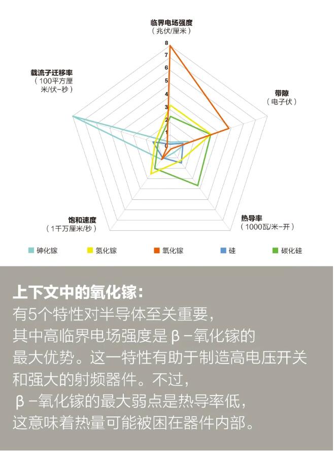

In his pioneering research, Towaki also introduced the situation that the power loss was greatly reduced due to the use of materials with high critical electric field strength. The electric field intensity is expressed by Ec, which is the real super power of gallium oxide. Simply put, if a material is placed between two conductors and the voltage is raised, then Ec is the electric field where the material begins to conduct electricity, and its conductivity is very strong, sometimes bringing disastrous consequences. The critical electric field strength of silicon is usually several hundred kilovolts per centimeter, while that of gallium oxide is 8 million volts per centimeter.
Of course, you can't have both. The critical electric field strength of the material determines how thin this area can be in the closed state. "Baliga figure of merit" is the key index of low-frequency power switching semiconductor, and it is named after B.Jayant Baliga, winner of IEEE Medal of Honor. Essentially, it represents the degree of reproduction of the details of the input signal by the output of the device at high voltage. This is a very important characteristic for a transistor that works as a switch in the frequency range of kilohertz. These devices are commonly found in multi-kV substation equipment, high-energy photon generators for medical imaging and power inverters for electric vehicles and industrial motor drivers. Gallium oxide has a natural advantage in such applications. At these frequencies, the figure of merit is proportional to the cube of the critical electric field strength. Therefore, high Ec means good merit. The fact behind the math is that this switch is either completely on or completely off most of the time, and rarely switches between the two. Therefore, most of the power loss only comes from the current resistance when the equipment is turned on. If the Ec value is high, thinner devices can be used, which means less resistance. The message conveyed by Dong Wei's research is very simple: a high-voltage switch with little loss at low frequency can be realized by using a strong and high electric field strength. Other teams soon understood this. In 2013, researchers developed a metal oxide semiconductor field effect transistor (MOSFET) with a breakdown voltage of 370 volts. In 2016, Wang Wenhai, who was working in the NICT Tohoku team at that time, increased the breakdown voltage to 750 volts with an additional structure called "field plating". Among these devices, gallium oxide is relatively easy to achieve high working voltage, which is quite remarkable. In just a few years, the research of this material has made great progress, while the research of gallium nitride took decades.
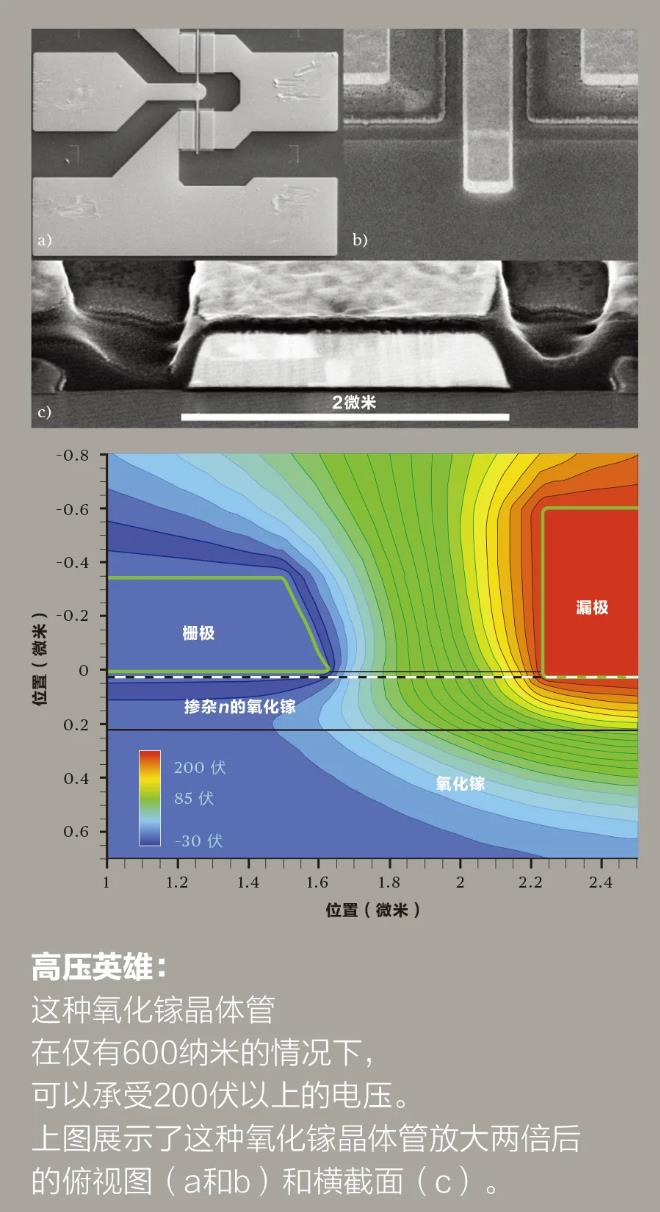
From the simple object of mobile phone charger, we can see the benefits of faster power switching speed. The working principle of the switch is to rectify the AC voltage of the wall plug first, and then chop it into a high-frequency signal. Reduce the transformer voltage to the required level, and finally rectify and filter the signal. The biggest part of the system is the transformer and other passive components. Only by increasing the frequency can smaller components be used. If a higher frequency is required, the semiconductor with wider band gap and higher critical electric field will help to achieve the goal more effectively, and at the same time simplify heat dissipation. For example, the switching power of a 1200-volt silicon inverter at a frequency of 20 kHz is about 3 kW. When switching at a frequency of 150 kHz, the silicon carbide inverter with the same power can work in a package with a size of only 1/3 at a higher temperature. Similar inverters based on gallium oxide can work at the same high temperature at a frequency close to megahertz, and the size can be reduced by half (although magnetic elements that have not yet been invented are required). Therefore, the real electronic properties of gallium oxide and other materials come from making full use of its critical electric field strength, but what is this critical electric field strength? Until 2015, no team has given the true number of field strength that this material can achieve. Like other devices, the preliminary results are far from the theoretical limit. My colleagues and I accepted this challenge while working in the U.S. Air Force Research Laboratory (AFRL) at Wright Patterson Air Force Base in Ohio. The first problem we have encountered is that any device made of materials with such high field strength may exceed the limit of available test equipment. In principle, a 2 micron material can block more than 1.5 kV! Therefore, we built a simple MOSFET, and reduced its geometric structure to suit the lower voltage. The gap between the gate and the drain (the position with the highest electric field) is only 600 nanometers. This is done partly to measure the peak value of Ec more conveniently, and also because we want to test the device at RF frequency (because larger high-voltage designs do not allow this). In this early research, the transistor can withstand 230 volts, which is the limit of RF test equipment. The resulting average electric field is at least 3.8 mv per cm, while the simulation shows that the peak value of the internal electric field is at least 5.3 mv per cm. Compared with the complete 8 megavolts per centimeter, we were surprised that such a large part was measured in the first attempt! This is the first time that the Ec value of gallium oxide is higher than the theoretical value of gallium nitride (about 3.3 mv per cm). Objectively speaking, the gate-drain gap of a GaN-like power transistor with a rated voltage of 600 volts is usually 15 to 20 microns, while ours is 600 nanometers. After obtaining this result, the research on power switching transistors began to develop at an alarming rate. In 2017, we manufactured MOSFET with breakdown voltage greater than 600 volts. At the beginning of 2018, MOSFET with different geometric structures achieved high-frequency loss values that reached or exceeded the theoretical limit of silicon. In addition, we now have a clear direction and can reach or exceed the most advanced gallium nitride value in the next few years.

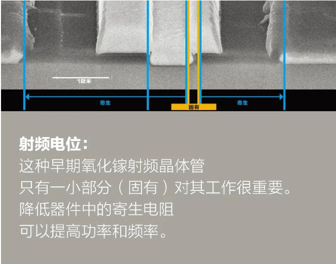
In transistors used to amplify RF signals, electron speed is particularly important. For RF technology, high power output and high frequency are the goals, which are summarized by JFOM. Johnson's figure of merit shows that the product of power and frequency of RF transistor is directly proportional to the product of the maximum carrier velocity in semiconductor material and Ec. The key is that in RF transistors, amplification can only be achieved when carriers can reach the drain from the source before the polarity of RF waveform is switched. The highest frequency at which this happens is called "Uniform Current Gain Frequency" (fT). Here, the high critical electric field of gallium oxide comes into play again, because you can narrow the critical distance, while still providing a strong electric field to accelerate the electrons to the highest speed. In 2017, we successfully developed the first sub-micron gallium oxide RF MOSFET in the US Air Force Research Laboratory. The data of these devices are impressive from the beginning, although they are not in the same level as those of gallium nitride. Their unified current gain frequency is 3 GHz and the maximum oscillation frequency is 13 GHz. At 800 MHz, the output power density is 230 milliwatts per millimeter. Later, the U.S. Air Force Research Laboratory also demonstrated that the output density of pulsed RF power exceeds 500 milliwatts per millimeter at 1 GHz, and the maximum oscillation frequency is close to 20 GHz. More encouragingly, at about the same time, Krishnendu Ghosh and Uttam Singisetti of the University of Buffalo published theoretical calculation results, which showed that JFOM of gallium oxide was obviously superior to gallium nitride. Since the first demonstration of its RF performance in 2017, the most significant progress made by RF gallium oxide technology is Sriram Krishnamoorthy and the new and improved doping technology developed by him and Siddharth Rajan of Ohio State University. These technologies draw lessons from silicon technology. In the semiconductors produced by these technologies, the resistance of the conductive material sheet is very low, about 300 ohms per square (this is the correct unit). This is comparable to the level in gallium nitride devices. Shortly after this result was obtained, Rajan and researchers at the University of California, Santa Barbara independently developed gallium oxide similar to high electron mobility transistor (HEMT). This kind of device is usually made of gallium arsenide (GaAs) or gallium nitride, and it is an important RF pillar for mobile phones and satellite TV receivers. This kind of device conducts electricity not through the doped channel of bulk semiconductor, but through the two-dimensional electron gas formed on the sharp interface between two semiconductors with different band gaps. The semiconductors in this case are aluminum gallium oxide and gallium oxide, which are completely similar to the commercial aluminum gallium arsenide/gallium arsenide HEMT technology in smart phones. These key breakthroughs are beneficial to the vertical and horizontal expansion of RF devices. Despite these promising developments, gallium oxide is unlikely to challenge the position of gallium arsenide or gallium nitride in all RF applications. Knowing that it is essentially a good switch, we hope that it will have advantages in switching mode amplifiers (such as Class D, Class E, or Class F). Among these amplifiers, the on-resistance of this device is very low during operation, and it can achieve very high efficiency by using the characteristics of low current and high breakdown voltage. On the other hand, gallium nitride will be favored for device applications requiring low impedance and high current, mainly because of its higher carrier mobility and carrier density.

So, what are the disadvantages of gallium oxide? The achilles heel of this material lies in its poor thermal conductivity. In fact, among all semiconductors that can be used for RF amplification or power switching, its thermal conductivity is the worst. The thermal conductivity of gallium oxide is only 1/60 of diamond, 1/10 of silicon carbide (the base of high-performance radio-frequency gallium nitride) and about 1/5 of silicon. (Interestingly, it is comparable to gallium arsenide, the main RF material. Low thermal conductivity means that the heat generated in the transistor may stay, which may greatly limit the lifetime of the device.

For example, researchers in Tokyo Laboratory of National Institute of Information and Communication Technology of Japan bonded P-type polycrystalline silicon carbide to the back of gallium oxide wafer about 10 microns thin, which greatly improved the thermal resistance of the device. Researchers in the U.S. Air Force Research Laboratory found that in some device topologies, almost all the heat is generated at the top of the material 1 micron, so they simulated the effect of contacting the electrode and using dielectric filler to divert heat to the radiator, and achieved good results. This is also the method used in commercial GaAs heterojunction bipolar transistors at present. Therefore, although gallium oxide has a thermal challenge, intelligent engineering design can overcome this problem.
Another more basic problem is that we can only make gallium oxide conduct electrons, but not holes. No one has ever made a good P-type conductor with gallium oxide. In addition, it is frustrating that the basic electronic characteristics of this material make it hopeless in this respect. In particular, the valence band part of the energy band structure of this material does not have the shape of hole conduction. Therefore, even if there is a dopant that can make the acceptor at the correct energy level, the generated holes will trap themselves before it helps conduction. When the theory is so consistent with the data, it is difficult to find a solution to this problem.
Although this weakness does bring more challenges, it is not an obstacle. Many so-called devices limited to most operators have also achieved commercial success, such as USB-C wall charger. The research stage of gallium oxide device technology has just begun to reach a critical scale. We are planning the application space of fast switches, multi-kV power transistors and RF devices. Nowadays, new kilovolt devices are often developed. Radio frequency transistors with critical dimensions of tens of nanometers are coming out soon. I very much hope that with the development of this technology, we can realize the device topology that was previously impossible in any other material.
Of course, we will break some things (mainly dielectrics) on the way to development, but this is the definition of disruptive technology. We exchange what we know for potential performance, but at present, the performance potential of gallium oxide is far greater than its problems.
Disclaimer: This article is reproduced from "EETOP". This article only represents the author's personal views, and does not represent the views of Sacco Micro and the industry. It is only for reprinting and sharing to support the protection of intellectual property rights. Please indicate the original source and author when reprinting. If there is any infringement, please contact us to delete it.
Company Tel: +86-0755-83044319
Fax/fax:+86-0755-83975897
Email: 1615456225@qq.com
QQ: 3518641314 Manager Li
QQ: 332496225 Manager Qiu
Address: Room 809, Block C, Zhantao Technology Building, No.1079 Minzhi Avenue, Longhua New District, Shenzhen
Related Recommendations





 粤公网安备44030002007346号