
























Service Hotline
News

News
Slkor 1SS181 Diode: 80V Withstand‑voltage, 0.3A, SOT‑23, High‑speed Switching Diode
2026-09-29
64
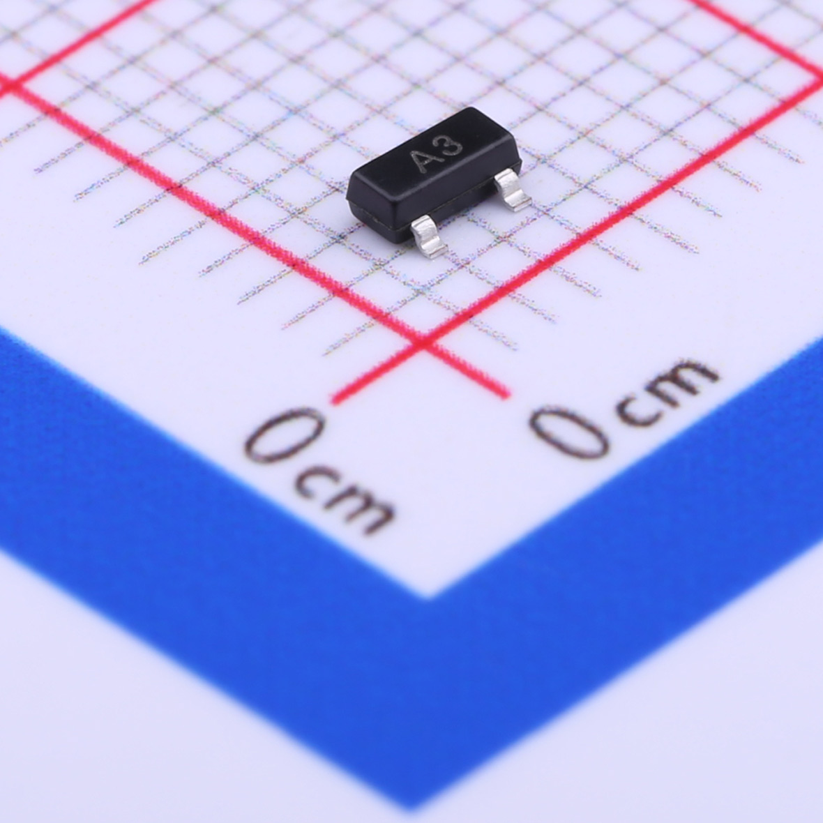
1SS181 is a high-speed switching diode in SOT-23 package with marking code A3. It features 80V DC reverse withstand-voltage and 300mA continuous forward current. It delivers low forward voltage drop and very short reverse recovery time, suitable for high-speed signal switching and low-current rectification applications. Based on the component datasheet, this document sorts out core parameters, key features, application fields and engineering design guidelines to provide reference for hardware component selection and circuit design.
About Slkor:
1. Core Product Parameters
Pin assignment: Pin 1-Cathode, Pin 2-Cathode, Pin 3-Anode. All electrical parameters are tested under reference ambient temperature of 25℃.
1.1 Absolute Maximum Ratings
- Non-repetitive peak reverse voltage: 85V - DC blocking voltage: 80V - Continuous forward current: 300mA - Average rectified output current: 100mA - Power dissipation: 150mW - Junction temperature: 125℃ - Storage temperature range: -55℃ ~ 125℃
1.2 Electrical Characteristics (Ambient temperature 25℃)
- Minimum reverse breakdown voltage 80V, test condition at reverse current 100μA - Forward voltage: typical value 0.61V at forward current 1mA; typical value 0.74V at forward current 10mA; typical value 0.92V and maximum 1.2V at forward current 100mA - Reverse leakage current: maximum 0.1μA under reverse voltage 30V; maximum 0.5μA under reverse voltage 80V - Total terminal capacitance: typical value 2.2pF, maximum 4.0pF, test condition reverse voltage 0V, frequency 1MHz - Reverse recovery time: typical value 1.6ns, maximum 4.0ns, test condition both forward current and reverse current equal to 10mA
1.3 Package and Marking Information
- Package type: SOT-23 - Device marking code: A3 - Pin assignment: Pin 1 Cathode, Pin 2 Cathode, Pin 3 Anode
2. Core Product Features
- Compact SOT-23 surface-mount package, compatible with automatic reflow soldering and saves PCB layout space.
- Low forward voltage drop under various forward-current operating conditions, which reduces conduction power loss.
- Short reverse recovery time with typical value of 1.6ns, providing excellent high-speed switching performance for high-frequency operating conditions.
- Low reverse leakage current reduces static power consumption and fits signal-processing circuits.
- Operating temperature ranges from -55℃ to 125℃, compatible with most temperature environments for consumer-electronic products.
3. Main Application Fields
- High-frequency signal switching circuits for one-way signal isolation and signal clamping.
- Low-current rectification circuits for signal-loop rectification with low power.
- Protection circuits for ESD and surge protection on IO ports and signal input terminals.
- Consumer-electronic equipment including remote controllers, portable devices and internal signal-processing loops of small home appliances.
- High-frequency analog circuits for high-frequency signal detection and amplitude-limiting processing.
4. Suggestions for Engineering Design
- Power and temperature management. The maximum power dissipation is 150mW. Actual power consumption during system operation shall not exceed rated value. Power derating is required when ambient temperature rises to prevent junction temperature from exceeding upper limit of 125℃.
- Safety margin for voltage and current. Actual reverse operating voltage shall not approach the 80V DC blocking-voltage limit. Do not apply reverse voltage higher than 85V non-repetitive peak value. Long-term operation at 300mA continuous forward-current limit should be avoided, and average rectified output current shall be kept within 100mA.
- High-speed switching application. This diode has good reverse-recovery-time performance. For high-frequency circuits, pay attention to high-frequency coupling effect brought by terminal capacitance.
- Influence of reverse leakage current. In high-impedance small-signal circuits, reverse leakage current may cause signal offset. Evaluate the impact of leakage current ranging from 0.1μA to 0.5μA on signal accuracy in design phase.
- Pin identification. Pin 1 and Pin 2 are both cathodes while Pin3 is anode. Verify pin definition during PCB footprint design and assembly to avoid device failure caused by reversed polarity.
- Parameter drift under temperature variation. Forward voltage and reverse leakage current change with ambient temperature. Reverse leakage current increases significantly under high temperature. Take performance shift caused by temperature-related parameter drift into consideration in system-level design.
5. Product Summary
1SS181 is a high-speed switching diode packaged in SOT-23, with 80V withstand-voltage and 300mA continuous forward current. It features low forward voltage drop and nanosecond-level reverse recovery time. It is suitable for high-frequency signal switching, low-current rectification, signal limiting and protection circuits. Hardware designers shall control actual power consumption, operating voltage and current with sufficient safety margin, and confirm pin polarity against reverse connection. Within absolute maximum ratings, the device can reliably realize functions including signal isolation, signal detection, low-current rectification and port protection.
About Slkor:
Slkor has research and development offices in Busan, South Korea, Beijing, China, and Suzhou, China. Most of the wafer manufacturing and packaging and testing are carried out within China. The company employs and collaborates with individuals and organizations worldwide, with a laboratory for product performance and reliability testing and a central warehouse located at its headquarters in Shenzhen. Slkor has filed for over a hundred invention patents, offers more than 2,000 product models, and serves over ten thousand customers globally. Its products are exported to countries and regions including Europe, the Americas, Southeast Asia, and the Middle East, making it one of the rapidly growing semiconductor companies in recent years. With well-established management systems and streamlined workflows, Slkor has rapidly enhanced the brand awareness and reputation of its "SLKOR" brand through its outstanding quality and standardized services. Its product range includes three major series: diodes, transistors, and power devices, with recent introductions of new products such as Hall elements and analog devices, expanding its presence in sensors, Risc-v microcontrollers, and other product categories.
Related Recommendations
Exclusive Interview with Li Gang of Yunfan Ruida: The Precision of Millimeter-Wave Radar Products and the Warmth of Humanity
2026-07-22
2551
RF Passion, Craftsman’s Journey: Over 30 Years of Steadfast Dedication — Interview with Kinghelm Chief Engineer Mr. Qin hongxiang
2026-06-26
2718





 粤公网安备44030002007346号